 ChipApex | Global Electronic Components Supplier
9FGV1002B207NBGI8
Search Product
Search Post
— IC芯片 | 连接器 | 传感器 | 被动器件 —
Search productSearch post
— IC芯片 | 连接器 | 传感器 | 被动器件 —
Consult the customer manager about the wholesale price.
consultation hotline:86-132-6715-2157
email:[email protected]
Contact the product manager for consultation. One-stop consultation is available.
Do you want a lower wholesale price? Please send us your inquiry and we will reply immediately.
The 9FGV1002B207NBGI8 is a programmable clock generator from Renesas' PhiClock™ family, designed for Ethernet and PCI Express applications. It features an integrated PLL and supports input signals via HCSL, LVCMOS, LVDS, or crystal. The device provides four spread-spectrum copies of a single output frequency and two copies of the crystal reference input. Output signaling options include CML, HCSL, LP-HCSL, LVCMOS, LVDS, and LVPECL. It operates within a temperature range of -40°C to 85°C and holds AEC-Q100 automotive qualification.
This component belongs to the 9FGV1002 series, which includes variants like 9FGV1002C000NBG2 and 9FGV1002C000NBGI. These devices share the core PhiClock™ architecture but differ in specific factory configurations, packaging (Tray vs. Reel), and suffix designations. The 9FGV1002B207NBGI8 represents a specific configuration within this family, distinguished by its ordering suffix and internal programming.
Configuration can be selected via hardware using two select pins or through software using two I²C bits. In I²C mode, any of the four OTP configurations can be set as the default.
The device accepts HCSL, LVCMOS, LVDS, or crystal inputs.
Yes, it is AEC-Q100 qualified and rated for an operating temperature range of -40°C to 85°C.
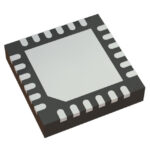 9FGV1002B207NBGI8
The activity of extra discounts on wholesale prices is in full swing…
Please fill in your contact information and we will send you the latest wholesale price list.






