 ChipApex | Global Electronic Components Supplier
9FGV1002BQ508LTGI
Search Product
Search Post
— IC芯片 | 连接器 | 传感器 | 被动器件 —
Search productSearch post
— IC芯片 | 连接器 | 传感器 | 被动器件 —
Consult the customer manager about the wholesale price.
consultation hotline:86-132-6715-2157
email:[email protected]
Contact the product manager for consultation. One-stop consultation is available.
Do you want a lower wholesale price? Please send us your inquiry and we will reply immediately.
The Renesas 9FGV1002BQ508LTGI is a PhiClock series clock generator IC designed for high-frequency timing applications. It operates within a supply voltage range of 1.71V to 1.89V, 2.375V to 2.625V, and 3.135V to 3.465V. The device supports input frequencies from 8MHz to 50MHz via crystal or LVCMOS sources. Output frequencies are programmable up to 200MHz and 325MHz. It features LP-HCSL, LVCMOS, and LVDS output signaling types with an output impedance of 100 ohms. The component utilizes a 24-LFLGA package with an exposed pad.
Verify the specific ordering suffix and package code against official Renesas documentation to ensure compatibility with design requirements. Confirm that the selected variant matches the required output signaling types and voltage levels. Cross-reference the manufacturer part number with authorized distributor catalogs to validate authenticity and current availability status before finalizing procurement plans.
Select this component when designing systems requiring precise clock synthesis for PCIe or Ethernet interfaces. Ensure the design accommodates the specified supply voltage ranges and input frequency constraints. Verify that the LFLGA package dimensions and thermal characteristics align with the target PCB layout and assembly processes. Consider the need for custom configuration tools if specific frequency outputs are required beyond standard configurations.
This device belongs to the Renesas PhiClock series, which provides programmable clock generation solutions. It is engineered to meet stringent jitter requirements for modern high-speed serial standards. The component integrates PLL technology to generate stable clock signals from lower-frequency inputs. It is suitable for applications demanding low phase noise and flexible output configurations in compact form factors.
Consult the official datasheet addendum for cross-reference information. Verify pinout compatibility and electrical specifications before substituting with other models in the 9FGV series. Ensure that any alternative component meets the same PCIe and Ethernet compliance standards.
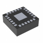 9FGV1002BQ508LTGI
The activity of extra discounts on wholesale prices is in full swing…
Please fill in your contact information and we will send you the latest wholesale price list.





