 ChipApex | Global Electronic Components Supplier
9FGV1002CQ505LTGI8
Search Product
Search Post
— IC芯片 | 连接器 | 传感器 | 被动器件 —
Search productSearch post
— IC芯片 | 连接器 | 传感器 | 被动器件 —
Consult the customer manager about the wholesale price.
consultation hotline:86-132-6715-2157
email:[email protected]
Contact the product manager for consultation. One-stop consultation is available.
Do you want a lower wholesale price? Please send us your inquiry and we will reply immediately.
The Renesas 9FGV1002CQ505LTGI8 is a PhiClock™ programmable clock generator designed for PCIe Gen1–7 applications. It features four spread-spectrum output pairs and two LVCMOS reference outputs, supporting frequencies up to 325MHz (LVDS/LP-HCSL) and 200MHz (LVCMOS). The device operates with core voltages of 1.8V or 3.3V and individual output supply options. It includes an integrated 50MHz crystal option and supports hardware or I²C configuration via select pins or software commands.
Verify the specific suffix LTGI8 against the official datasheet to confirm package type and configuration. Confirm availability status as inventory levels fluctuate. Ensure compatibility with required I/O voltage standards before procurement.
Select this component when PCIe Gen7 low jitter requirements are critical. Choose based on required output signaling standards (LP-HCSL vs LVDS). Verify that the 1:6 input-to-output ratio meets system topology needs. Check if the integrated crystal option simplifies board design compared to external crystals.
This part belongs to the Renesas PhiClock™ family of programmable clock generators. It is specifically engineered for high-speed serial interface timing, offering flexibility in frequency generation and output formatting for complex multi-lane architectures.
Direct substitutes within the same family include 9FGV1002C000NBG2 and 9FGV1002CQ501LTGI8. Verify pinout and configuration settings match exactly when swapping between variants.
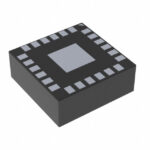 9FGV1002CQ505LTGI8
The activity of extra discounts on wholesale prices is in full swing…
Please fill in your contact information and we will send you the latest wholesale price list.





