 ChipApex | Global Electronic Components Supplier
9FGV1004B206NBGI8
Search Product
Search Post
— IC芯片 | 连接器 | 传感器 | 被动器件 —
Search productSearch post
— IC芯片 | 连接器 | 传感器 | 被动器件 —
Consult the customer manager about the wholesale price.
consultation hotline:86-132-6715-2157
email:[email protected]
Contact the product manager for consultation. One-stop consultation is available.
Do you want a lower wholesale price? Please send us your inquiry and we will reply immediately.
The Renesas 9FGV1004B206NBGI8 is a programmable PhiClock generator from the 9FGV1004 family, designed for high-performance timing applications. It features four differential output pairs supporting LP-HCSL and LVDS signaling standards, alongside two LVCMOS reference outputs. The device operates with core voltages of 1.8V or 3.3V and supports I/O voltages ranging from 1.8V to 3.3V per output pair. It delivers typical RMS phase jitter of 267fs at 156.25MHz (12kHz–20MHz bandwidth) and complies with PCIe Gen1 through Gen4 specifications. The component is housed in a compact 4x4mm 24-VFQFPN package.
Verify the specific suffix 'B206' against official Renesas documentation to confirm factory configuration details. Confirm the '8' suffix indicates reel packaging if required for assembly processes. Ensure compatibility with the 24-VFQFPN footprint during procurement planning.
Select this model when PCIe Gen1-4 compliance and low jitter are required. Choose between LP-HCSL or LVDS based on downstream receiver requirements. Verify that the 1.8V or 3.3V core voltage aligns with the system power architecture. Consider I²C control needs versus hardware pin selection for configuration flexibility.
This part belongs to the Renesas PhiClock™ programmable clock generator family. The 9FGV1004 series provides flexible clock distribution solutions with multiple output configurations. It is distinct from the 9FGV1001 and 9FGV1002 series by offering mixed integer/fractional output capabilities and specific jitter performance metrics tailored for modern serial link standards.
Direct replacements within the same family include other 9FGV1004 variants with different output frequencies or packaging options. Cross-family substitution requires careful evaluation of jitter specifications and output drive strength compatibility.
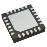 9FGV1004B206NBGI8
The activity of extra discounts on wholesale prices is in full swing…
Please fill in your contact information and we will send you the latest wholesale price list.





