 ChipApex | Global Electronic Components Supplier
9FGV1004B215NBGI
Search Product
Search Post
— IC芯片 | 连接器 | 传感器 | 被动器件 —
Search productSearch post
— IC芯片 | 连接器 | 传感器 | 被动器件 —
Consult the customer manager about the wholesale price.
consultation hotline:86-132-6715-2157
email:[email protected]
Contact the product manager for consultation. One-stop consultation is available.
Do you want a lower wholesale price? Please send us your inquiry and we will reply immediately.
The Renesas 9FGV1004B215NBGI is a programmable clock generator from the PhiClock family, designed for high-performance timing applications. It features four differential output pairs supporting LP-HCSL and LVDS signaling standards. The device operates within a supply voltage range of 1.71 V to 3.465 V and supports output frequencies up to 325 MHz. Key electrical specifications include a maximum input frequency of 240 MHz and a typical phase jitter of 27 ps. It is housed in a compact 24-pin VFQFPN package with dimensions of 4.0 mm x 4.0 mm.
Verify component authenticity through authorized Renesas distributors. Confirm the specific suffix 'NBGI' corresponds to the 24-VFQFPN tray packaging format. Check for end-of-life status or alternative recommendations if current stock is limited. Ensure compatibility with existing PCB footprints and thermal requirements for the VFQFPN-24 package.
Select this model when four independent differential clock outputs are required with flexible signaling standards. The 9FGV1004 series allows configuration via two select pins or I²C, offering flexibility for multi-unit systems with unique addresses. Verify that the required output frequency falls within the 1 MHz to 325 MHz range and that the power supply constraints align with the 1.71 V to 3.465 V operating window.
This component belongs to the Renesas PhiClock™ programmable clock generator family, which includes variants like the 9FGV1001, 9FGV1002, and 9FGV1008. These devices share common architectural features such as I²C configurability and support for PCIe jitter compliance. The 9FGV1004 specifically provides a mix of integer-related and fractional/spread-spectrum outputs, distinguishing it from models with uniform output types.
Direct replacements within the same family include other 9FGV1004 variants with different output frequencies or packaging suffixes (e.g., LTGI for LGA). Cross-family substitution requires careful evaluation of pin compatibility and electrical parameters.
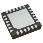 9FGV1004B215NBGI
The activity of extra discounts on wholesale prices is in full swing…
Please fill in your contact information and we will send you the latest wholesale price list.






