 ChipApex | Global Electronic Components Supplier
9FGV1004B219NBGI
Search Product
Search Post
— IC芯片 | 连接器 | 传感器 | 被动器件 —
Search productSearch post
— IC芯片 | 连接器 | 传感器 | 被动器件 —
Consult the customer manager about the wholesale price.
consultation hotline:86-132-6715-2157
email:[email protected]
Contact the product manager for consultation. One-stop consultation is available.
Do you want a lower wholesale price? Please send us your inquiry and we will reply immediately.
The Renesas 9FGV1004B219NBGI is a programmable clock generator from the PhiClock family, designed for high-performance timing applications. It features four differential output pairs supporting LP-HCSL and LVDS signaling standards. The device operates within a supply voltage range of 1.71 V to 3.465 V and supports input frequencies up to 240 MHz, with maximum output frequencies reaching 325 MHz. Key electrical specifications include a typical phase jitter of 27 ps and a duty cycle of up to 60%. Packaged in a compact VFQFPN-24 format, it is suitable for systems requiring precise clock distribution.
This component is listed as obsolete or end-of-life by the manufacturer. Availability is limited to existing stock or third-party distributors. Verify current lifecycle status and lead times carefully before design-in. No direct replacement is officially confirmed in public documentation; evaluate pin-compatible alternatives if necessary.
Select this part when four independent differential clocks are required with flexible output voltage levels (1.8V/3.3V). Ensure the application supports I²C configuration or hardware pin selection. Confirm that the input crystal frequency matches the device's supported range. Check PCB layout guidelines for VFQFPN-24 package thermal and signal integrity requirements.
Part of the Renesas PhiClock 9FGV1004 series, which offers configurable clock generation solutions. The 'B' suffix typically denotes specific factory programming or revision details. This model is distinct from other variants like 9FGV1004BQ500LTGI by its unique output frequency configuration programmed at manufacture.
No publicly confirmed direct substitute part numbers are available in official documentation. Consider evaluating other members of the 9FGV1004 family or newer Renesas clock generators with similar pinouts and electrical characteristics. Perform full functional and timing verification if substituting.
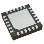 9FGV1004B219NBGI
The activity of extra discounts on wholesale prices is in full swing…
Please fill in your contact information and we will send you the latest wholesale price list.





