ChipApex | Global Electronic Components Supplier
9FGV1005A099LTGI
Search Product
Search Post
— IC芯片 | 连接器 | 传感器 | 被动器件 —
Search productSearch post
— IC芯片 | 连接器 | 传感器 | 被动器件 —
Consult the customer manager about the wholesale price.
consultation hotline:86-132-6715-2157
email:[email protected]
Contact the product manager for consultation. One-stop consultation is available.
Do you want a lower wholesale price? Please send us your inquiry and we will reply immediately.
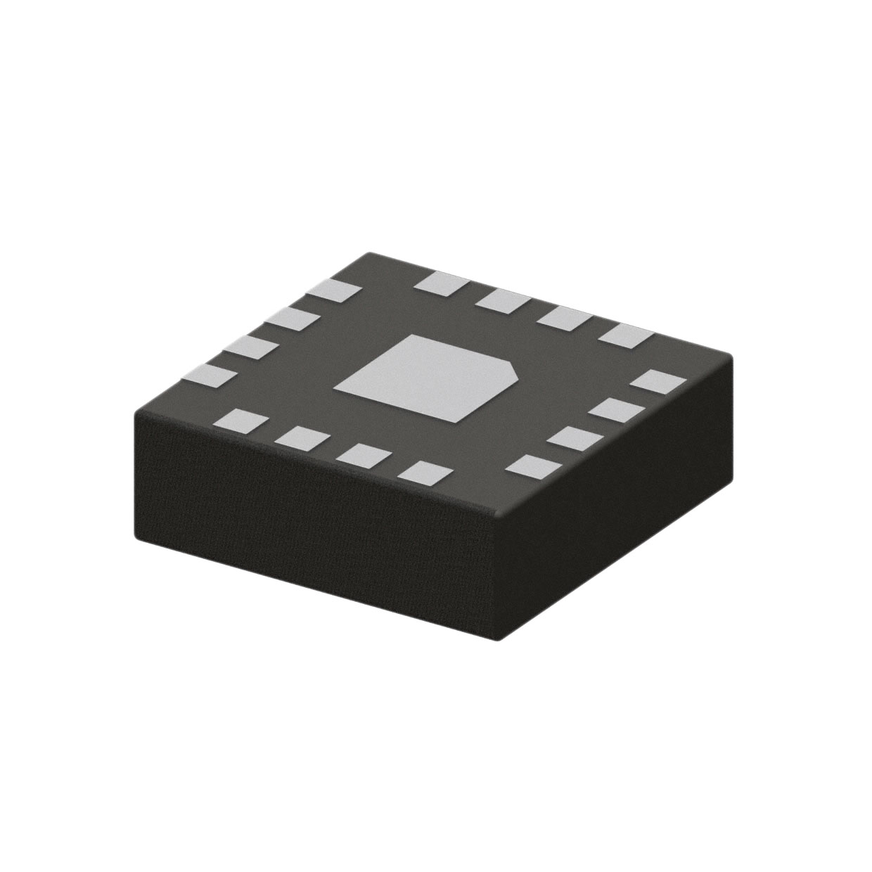
The 9FGV1005A099LTGI is a PhiClock programmable clock generator manufactured by Renesas Electronics. It operates within a supply voltage range of 1.71V to 3.465V and supports an input frequency of up to 325MHz. The device features one circuit with a 1:4 input-to-output ratio, providing four output signals. It accommodates various input formats including HCSL, LVCMOS, LVDS, and crystals, while supporting outputs such as HCSL, LVCMOS, LVDS, and LVPECL. Designed for surface mount installation in a 16-TFLGA package with an exposed pad, it functions reliably across a temperature range of -40°C to 85°C.
Verify the specific suffix LTGI against official Renesas documentation to confirm package type and moisture sensitivity level. Ensure compatibility with required input/output voltage levels and signal standards before integration. Confirm availability through authorized distributors as lead times may vary. Check for any recent product change notices regarding assembly locations or material compliance updates.
Select this component when a single-input, four-output clock generator is required for high-speed digital interfaces. Consider the 16-TFLGA package size for space-constrained designs. Verify that the supported input frequencies and output drive strengths meet the target application's jitter and impedance requirements. Ensure the operating temperature range aligns with the environmental conditions of the final system.
This part belongs to the Renesas PhiClock™ family of programmable clock generators. These devices are designed to provide low-jitter clock signals for high-performance digital systems. The 9FGV1005 series specifically targets applications requiring flexible clock configuration and multiple output drivers from a single reference source.
It supports HCSL, LVCMOS, LVDS, and crystal inputs.
Yes, Renesas PhiClock devices are typically RoHS compliant; verify the specific datasheet for confirmation.
Yes, the device allows configuration via hardware select pins or I²C interface during operation.
 9FGV1005A099LTGI
The activity of extra discounts on wholesale prices is in full swing…
Please fill in your contact information and we will send you the latest wholesale price list.