ChipApex | Global Electronic Components Supplier
9FGV1005A114LTGI8
Search Product
Search Post
— IC芯片 | 连接器 | 传感器 | 被动器件 —
Search productSearch post
— IC芯片 | 连接器 | 传感器 | 被动器件 —
Consult the customer manager about the wholesale price.
consultation hotline:86-132-6715-2157
email:[email protected]
Contact the product manager for consultation. One-stop consultation is available.
Do you want a lower wholesale price? Please send us your inquiry and we will reply immediately.
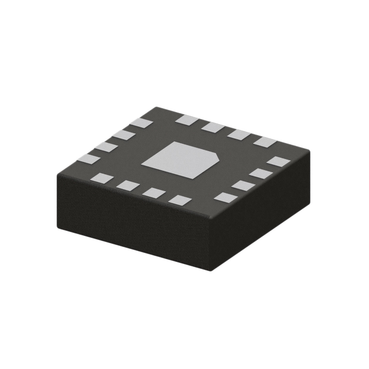
The 9FGV1005A114LTGI8 is a programmable clock generator IC from the PhiClock series, manufactured by Renesas Electronics. It operates within a supply voltage range of 1.71 V to 3.465 V and supports maximum output frequencies up to 325 MHz. The device features a single circuit configuration with one input and four outputs, utilizing a 1:4 input-to-output ratio. It is housed in a 16-TFLGA package with an exposed pad, designed for surface-mount installation. The component functions as a PLL-based clock generator, supporting various input types including HCSL, LVCMOS, LVDS, and crystals.
Verify the specific suffix LTGI8 against official Renesas documentation to confirm package type and tape-and-reel specifications. Ensure compatibility with required input/output signal standards such as HCSL or LVDS before integration. Cross-reference the part number with authorized distributors to confirm current availability and manufacturing status, as supply chain conditions may vary.
Select this component when a single-input, four-output clock distribution solution is required with frequencies up to 325 MHz. Consider the 16-TFLGA package constraints and thermal requirements associated with the exposed pad design. Evaluate the need for programmability versus fixed-frequency alternatives within the PhiClock family based on system flexibility requirements.
This part belongs to the 9FGV1005 series of programmable clock generators. It shares architectural similarities with other variants like the 9FGV1005Q500LTGI but differs in specific frequency configurations and output ratios. The series is designed for applications demanding low jitter and flexible clock generation in compact form factors.
The 9FGV1005A004LTGI is listed as a related variant within the same product line. Verify pinout compatibility and electrical parameter alignment before substitution. Other parts in the 9FGV1005 series may offer different output counts or frequency ranges.
 9FGV1005A114LTGI8
The activity of extra discounts on wholesale prices is in full swing…
Please fill in your contact information and we will send you the latest wholesale price list.