ChipApex | Global Electronic Components Supplier
9FGV1005A204LTGI8
Search Product
Search Post
— IC芯片 | 连接器 | 传感器 | 被动器件 —
Search productSearch post
— IC芯片 | 连接器 | 传感器 | 被动器件 —
Consult the customer manager about the wholesale price.
consultation hotline:86-132-6715-2157
email:[email protected]
Contact the product manager for consultation. One-stop consultation is available.
Do you want a lower wholesale price? Please send us your inquiry and we will reply immediately.
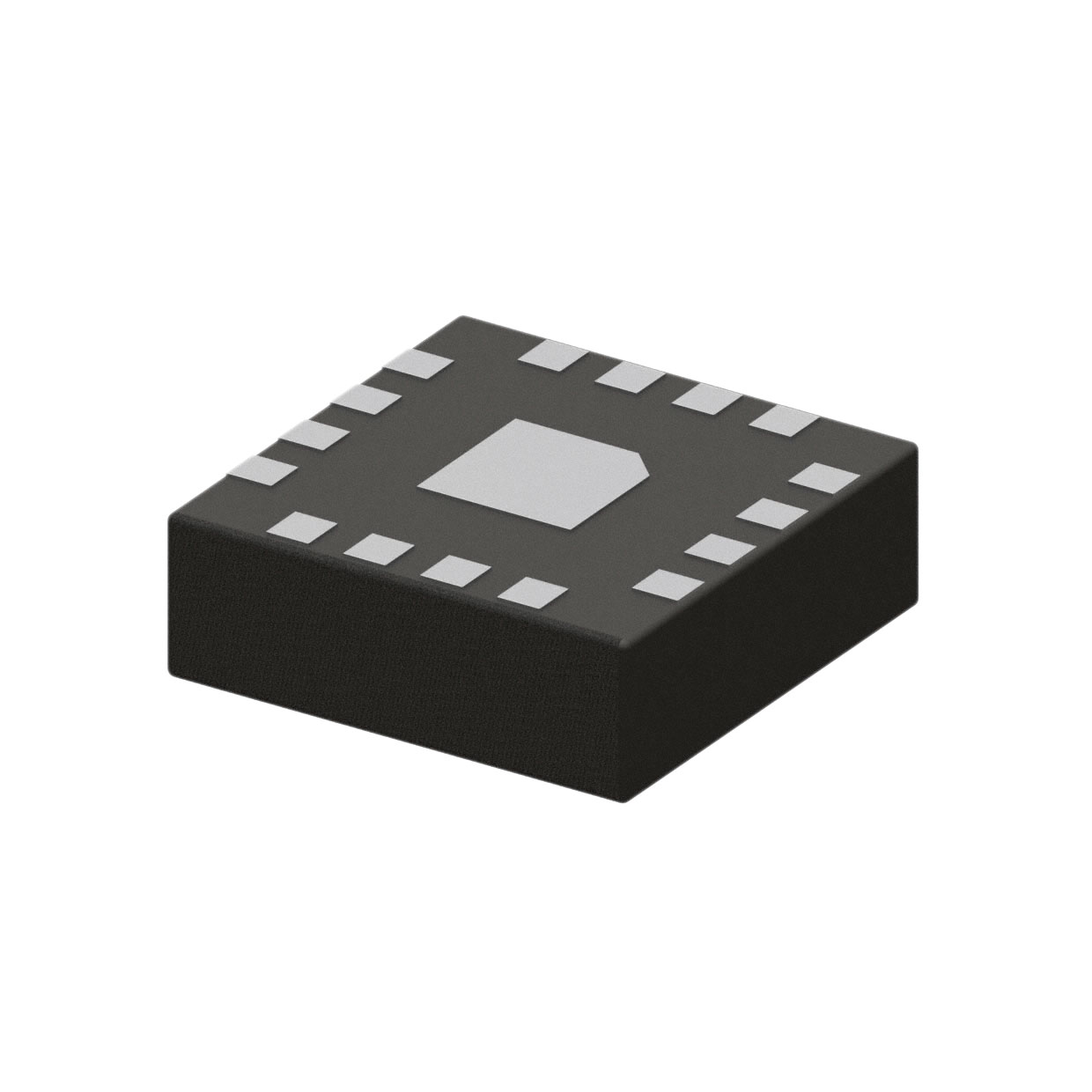
The 9FGV1005A204LTGI8 is a programmable clock generator from the Renesas PhiClock family, designed for low phase noise applications. It operates on a single supply voltage ranging from 1.8 V to 3.3 V and features one input channel with two differential outputs supporting LP-HCSL and LVDS signaling types. The device utilizes a 16-TFLGA package with an exposed pad, measuring 4.0 x 4.0 mm with a height of 1.4 mm. It supports crystal or LVCMOS inputs and includes spread spectrum capabilities. The component functions within a temperature range of -40°C to 85°C and complies with jitter requirements for PCIe Gen1 through Gen4 standards.
Verify the specific suffix LTGI8 against official Renesas documentation to confirm package type and tape-and-reel specifications. Ensure the ordering part number matches the required frequency configuration and output drive strength. Confirm moisture sensitivity level and reflow soldering profile requirements prior to assembly. Cross-reference the exact part number with the manufacturer's current production status to avoid obsolete components.
Select this component when low jitter performance is critical for PCIe or similar high-speed serial interfaces. Choose based on the requirement for dual differential outputs in LP-HCSL or LVDS formats. Consider the 1.8 V to 3.3 V operating voltage range for compatibility with existing system power rails. Evaluate the 16-TFLGA package dimensions for PCB space constraints and thermal dissipation needs.
This model belongs to the 9FGV1005C series of programmable clock generators, optimized for low phase noise. It shares architectural similarities with other PhiClock devices but offers specific pinout and configuration options. The series is designed to replace fixed-frequency oscillators in systems requiring precise timing adjustments and jitter cleaning capabilities for modern digital interfaces.
Check the 9FGV1005C series datasheet for direct functional equivalents. Verify pin-to-pin compatibility and electrical parameter alignment before substitution.
 9FGV1005A204LTGI8
The activity of extra discounts on wholesale prices is in full swing…
Please fill in your contact information and we will send you the latest wholesale price list.