ChipApex | Global Electronic Components Supplier
9FGV1006A204LTGI8
Search Product
Search Post
— IC芯片 | 连接器 | 传感器 | 被动器件 —
Search productSearch post
— IC芯片 | 连接器 | 传感器 | 被动器件 —
Consult the customer manager about the wholesale price.
consultation hotline:86-132-6715-2157
email:[email protected]
Contact the product manager for consultation. One-stop consultation is available.
Do you want a lower wholesale price? Please send us your inquiry and we will reply immediately.
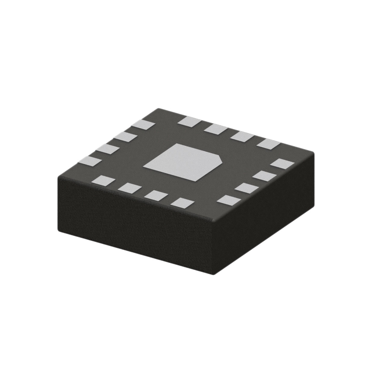
The 9FGV1006A204LTGI8 is a programmable clock generator from Renesas Electronics' PhiClock™ family. It operates within a supply voltage range of 1.71V to 1.89V, 2.375V to 2.625V, and 3.135V to 3.465V. The device features one input and six outputs with a 1:6 ratio. Output signaling supports CML, HCSL, LP-HCSL, LVCMOS, LVDS, and LVPECL standards. Maximum frequencies reach 200MHz and 325MHz. It utilizes an internal PLL for frequency synthesis and accepts HCSL, LVCMOS, LVDS, or crystal inputs. The component is housed in a 16-TFLGA package with an exposed pad.
Verify the specific suffix LTGI8 against the manufacturer's current datasheet to confirm pinout and electrical characteristics. Check for product change notices regarding assembly locations or material declarations. Confirm moisture sensitivity level (MSL) handling requirements prior to surface mount placement. Ensure the ordering quantity matches the standard carrier type specifications provided by authorized distributors.
Select this component when multiple distinct clock domains are required from a single reference source. Verify that the available output voltage levels match the receiving logic families. Consider the thermal performance of the 16-LGA(3x3) package for the target application environment. Compare jitter performance metrics against the specific requirements of the downstream high-speed serial links.
This part belongs to the 9FGV1006 series, which includes variants like the 9FGV1006Q550LTGI8. These devices share the PhiClock™ platform designed for low-jitter clock generation. The series is commonly used in infrastructure equipment requiring precise timing synchronization across multiple buses and peripherals.
Direct substitutes include other 9FGV1006 series variants such as 9FGV1006Q550LTGI8 if pin-compatible and electrically equivalent. Cross-reference the specific output configuration and frequency ranges before substitution.
 9FGV1006A204LTGI8
The activity of extra discounts on wholesale prices is in full swing…
Please fill in your contact information and we will send you the latest wholesale price list.