ChipApex | Global Electronic Components Supplier
9FGV1006A205LTGI8
Search Product
Search Post
— IC芯片 | 连接器 | 传感器 | 被动器件 —
Search productSearch post
— IC芯片 | 连接器 | 传感器 | 被动器件 —
Consult the customer manager about the wholesale price.
consultation hotline:86-132-6715-2157
email:[email protected]
Contact the product manager for consultation. One-stop consultation is available.
Do you want a lower wholesale price? Please send us your inquiry and we will reply immediately.
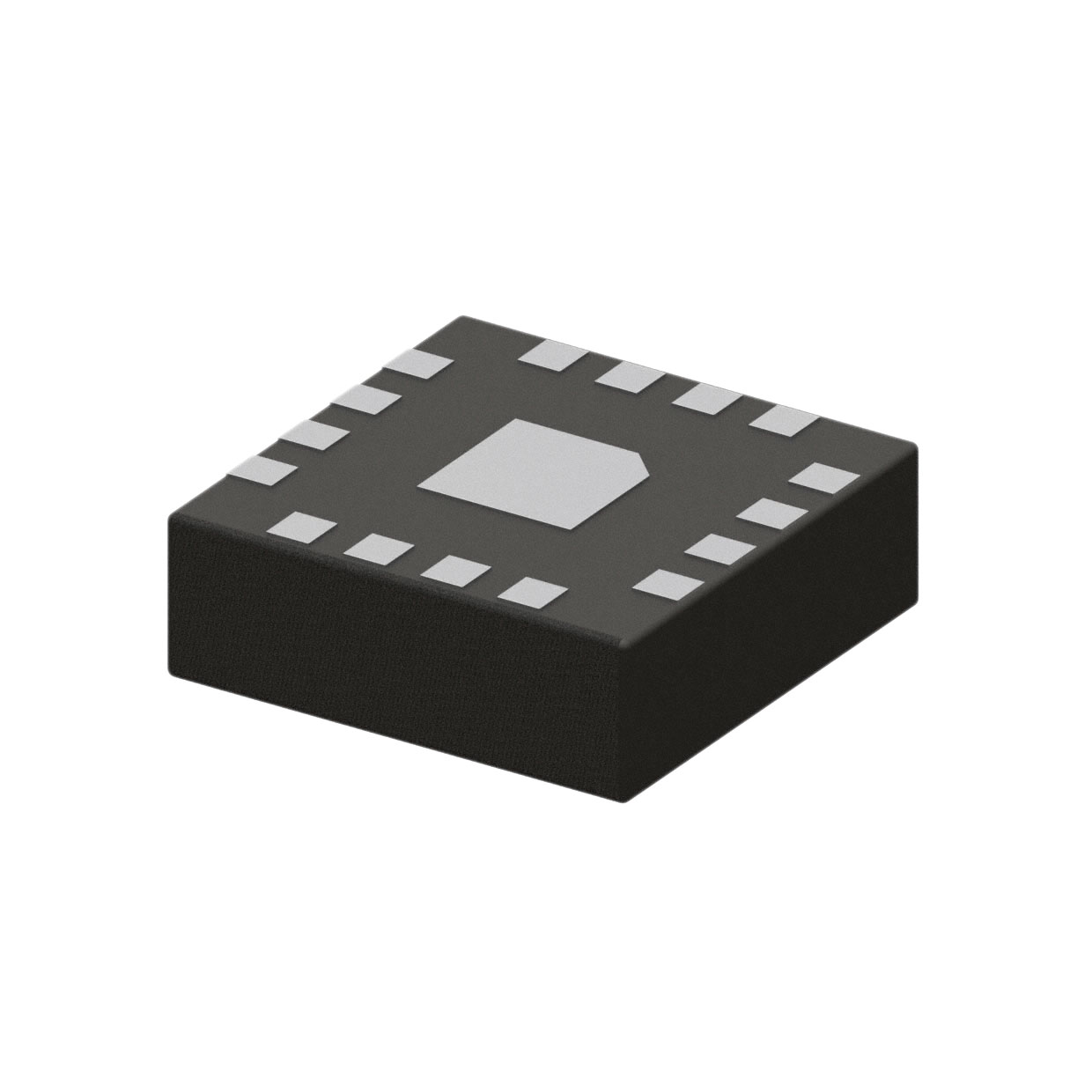
The 9FGV1006A205LTGI8 is a programmable clock generator from the Renesas PhiClock family, designed for high-performance timing applications. It features an integrated Phase-Locked Loop (PLL) and supports multiple input/output configurations including LVCMOS, HCSL, and LVDS signaling. The device operates within a supply voltage range of 1.71V to 3.465V and functions across a temperature range of -40°C to 85°C. Key electrical parameters include maximum output frequencies up to 325MHz and common-mode jitter performance suitable for PCIe Gen1 through Gen4 standards.
Verify the specific suffix 'A205' against official Renesas documentation to confirm factory-programmed frequency settings and pinout compatibility. Confirm moisture sensitivity level (MSL 3) handling requirements during assembly. Check for end-of-life notices or alternative package availability as this component type may have superseded variants in current production lines.
Select this model when fixed-frequency, factory-programmed clock generation is required without external programming hardware. Ensure the required output voltage levels (1.8V or 3.3V) match the target logic families. Verify that the 16-TFLGA package dimensions fit the PCB layout constraints compared to other PhiClock family members like the 9FGV1004 or 9FGV1008.
This part belongs to the 9FGV1006 series, which offers six outputs. It differs from the 9FGV1005 (five outputs) and 9FGV1004 (four outputs) primarily in output count and specific pin assignments. The 'LTGI8' suffix indicates a tape-and-reel packaging format with lead-free termination, distinct from tray-packaged variants like the 9FGV1006C000LTGI.
Direct substitutes include other 9FGV1006 variants with matching output frequencies if the A205 configuration is not critical. For pin-compatible upgrades, consider the 9FGV1008 series for additional outputs or the 9FGV1005 series for reduced pin counts. Always verify electrical parameter equivalence before substitution.
 9FGV1006A205LTGI8
The activity of extra discounts on wholesale prices is in full swing…
Please fill in your contact information and we will send you the latest wholesale price list.