ChipApex | Global Electronic Components Supplier
9FGV1006BQ532LTGI8
Search Product
Search Post
— IC芯片 | 连接器 | 传感器 | 被动器件 —
Search productSearch post
— IC芯片 | 连接器 | 传感器 | 被动器件 —
Consult the customer manager about the wholesale price.
consultation hotline:86-132-6715-2157
email:[email protected]
Contact the product manager for consultation. One-stop consultation is available.
Do you want a lower wholesale price? Please send us your inquiry and we will reply immediately.
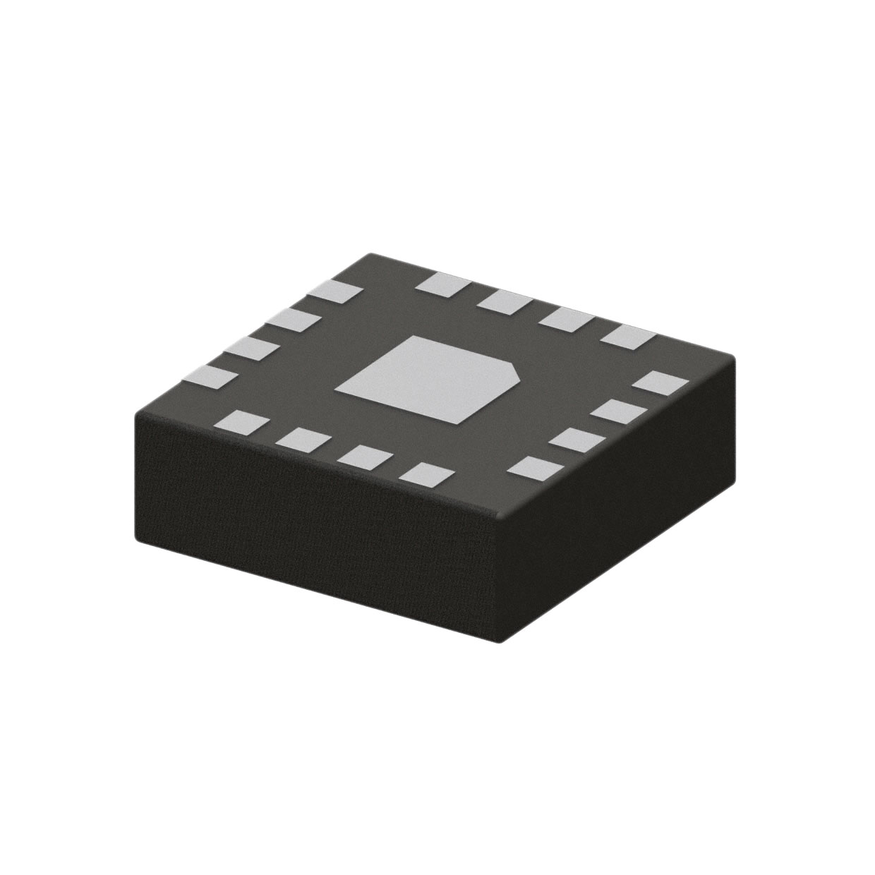
The Renesas 9FGV1006BQ532LTGI8 is a PhiClock™ programmable clock generator IC housed in a 16-TFLGA exposed pad package. It features a single circuit with a 1:3 input-to-output ratio and supports differential outputs. The device accepts HCSL, LVCMOS, LVDS, or crystal inputs to generate outputs compliant with HCSL, LVCMOS, LVDS, and LVPECL standards. Maximum operating frequency reaches 325MHz. Supply voltages include ranges of 1.71V–1.89V, 2.375V–2.625V, and 3.135V–3.465V. It operates within a temperature range of -40°C to 85°C.
Verify the specific suffix LTGI8 against official Renesas documentation to confirm tape-and-reel packaging and lead finish specifications. Confirm availability status as distribution listings may vary. Ensure ESD handling protocols are followed due to surface mount construction.
Select this component when a 1:3 clock distribution ratio is required with mixed standard output support. Verify that the 16-LGA (3x3) footprint fits the PCB layout constraints. Ensure supply voltage rails match the specified 1.8V, 2.5V, or 3.3V domains for proper operation.
This part belongs to the Renesas PhiClock™ series, designed for low-jitter clock generation. It shares architectural similarities with other 9FGV100x models but differs in pin count and output configuration capabilities specific to the 16-pin LGA form factor.
Check for direct cross-reference parts within the 9FGV1006 series. Evaluate alternative packages if 16-LGA sourcing is limited, ensuring electrical compatibility and thermal performance remain consistent.
 9FGV1006BQ532LTGI8
The activity of extra discounts on wholesale prices is in full swing…
Please fill in your contact information and we will send you the latest wholesale price list.