ChipApex | Global Electronic Components Supplier
9FGV1006C001LTGI
Search Product
Search Post
— IC芯片 | 连接器 | 传感器 | 被动器件 —
Search productSearch post
— IC芯片 | 连接器 | 传感器 | 被动器件 —
Consult the customer manager about the wholesale price.
consultation hotline:86-132-6715-2157
email:[email protected]
Contact the product manager for consultation. One-stop consultation is available.
Do you want a lower wholesale price? Please send us your inquiry and we will reply immediately.
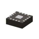
The 9FGV1006C001LTGI is a programmable PhiClock generator manufactured by Renesas Electronics. It provides four non-spread-spectrum copies of a single output frequency and two copies of the crystal reference input. The device supports hardware selection via select pins or software configuration through I²C, allowing users to define default configurations in OTP memory. It features four unique I²C addresses for multi-component access. The component operates within an industrial temperature range of -40°C to 85°C and utilizes a 24-lead LGA package with dimensions of 4.0 x 4.0 x 1.4 mm.
Verify the specific suffix LTGI against official Renesas documentation to confirm the lead finish (e4 Au) and moisture sensitivity level (MSL 3). Confirm the factory-configured nature of the part, as it requires ordering through authorized channels using the custom part configuration tool rather than standard off-the-shelf inventory.
Select this model when four identical non-spread-spectrum clock signals are required alongside two reference inputs. Ensure the design accommodates the 24-lead LGA footprint (4.0 x 4.0 x 1.4 mm). Verify that the target application supports the specified PCIe generation jitter compliance requirements and operates within the -40°C to 85°C temperature range.
This component belongs to the 9FGV1006 series within the PhiClock family of programmable clock generators. It shares architectural similarities with other models in the series, such as the 9FGV1004 and 9FGV1005, but is distinguished by its specific output count and non-spread-spectrum configuration capabilities for high-speed serial interface applications.
Direct replacements within the same family include the 9FGV1004CQ501LTGI8 and 9FGV1005 variants. Verify pin compatibility and output signaling types (LP-HCSL/LVDS) before substitution, as package types and output counts may differ across the series.
 9FGV1006C001LTGI
The activity of extra discounts on wholesale prices is in full swing…
Please fill in your contact information and we will send you the latest wholesale price list.