ChipApex | Global Electronic Components Supplier
9FGV1006C115LTGI8
Search Product
Search Post
— IC芯片 | 连接器 | 传感器 | 被动器件 —
Search productSearch post
— IC芯片 | 连接器 | 传感器 | 被动器件 —
Consult the customer manager about the wholesale price.
consultation hotline:86-132-6715-2157
email:[email protected]
Contact the product manager for consultation. One-stop consultation is available.
Do you want a lower wholesale price? Please send us your inquiry and we will reply immediately.
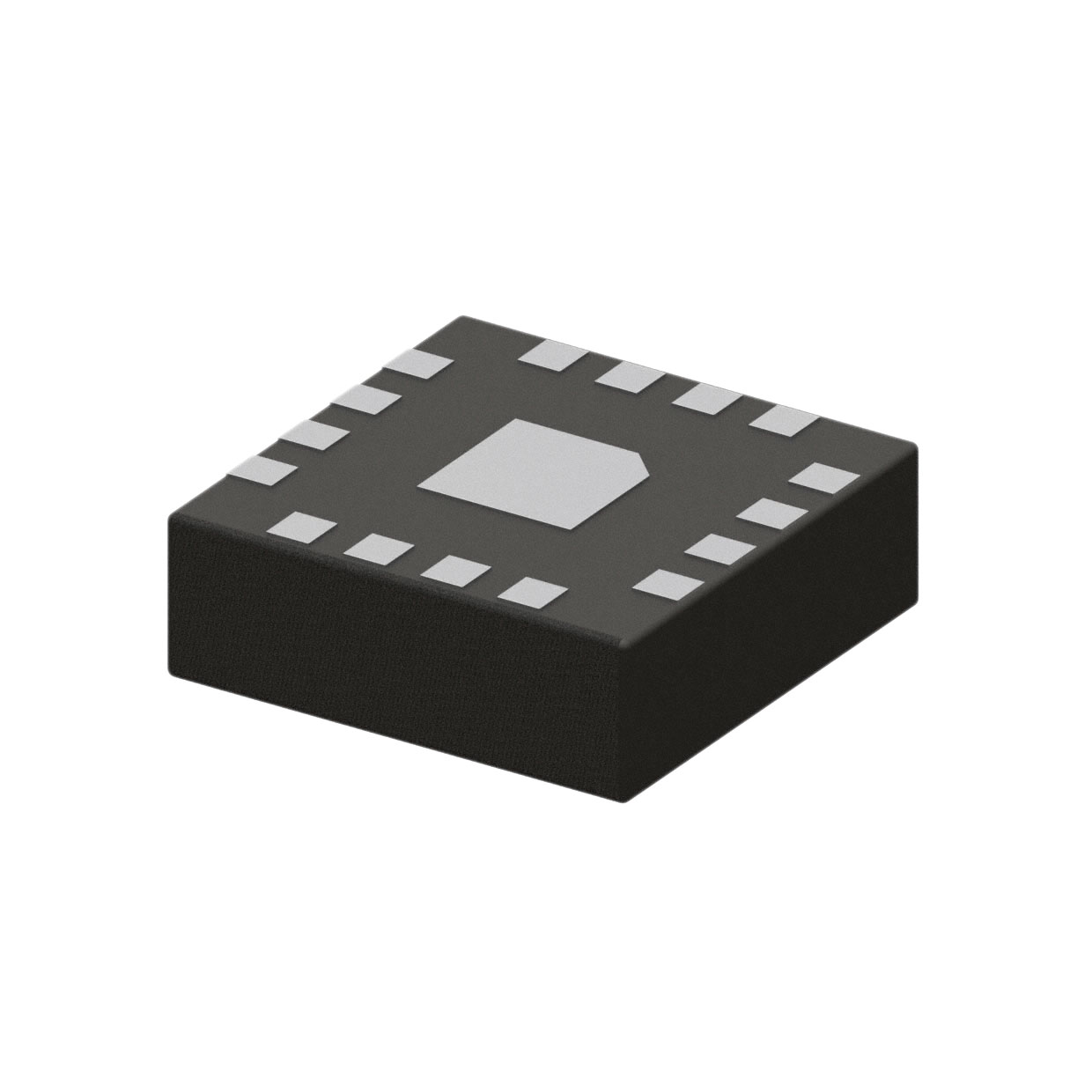
The 9FGV1006C115LTGI8 is a programmable PhiClock™ clock generator IC manufactured by Renesas Electronics Corporation. It operates within the 9FGV1006C series and utilizes a 16-TFLGA exposed pad package with surface mount installation. The device supports multiple supply voltage ranges, specifically 1.71V to 1.89V, 2.375V to 2.625V, and 3.135V to 3.465V. It features a PLL architecture with one circuit capable of generating outputs from a single input. Maximum output frequencies reach 200MHz and 325MHz. The component is designed for operation across an ambient temperature range of -40°C to 85°C.
Verify component status prior to procurement as specific suffixes may indicate end-of-life or obsolescence. Confirm moisture sensitivity level (MSL 3) and reflow soldering profiles during handling. Ensure I²C address configuration matches system requirements to prevent bus conflicts when deploying multiple units. Validate that the 16-TFLGA package dimensions align with the target PCB footprint design.
Select this model when a single-input, multi-output clock generator is required for high-speed serial interfaces. Choose based on the necessary output signaling standards, such as LVDS or LP-HCSL, to match downstream logic families. Verify that the available supply voltage rails correspond to the device's specified operating ranges. Consider the I²C configurability if dynamic frequency adjustment or default OTP configuration selection is needed in the final application.
This part belongs to the Renesas PhiClock™ family of programmable clock generators. The 9FGV1006C variant typically offers six outputs derived from one input, supporting ratios like 1:6. It is engineered for low jitter performance suitable for PCIe and Ethernet applications. The LTGI8 suffix denotes the specific 16-lead TFLGA package with an exposed thermal pad, distinguishing it from other package options in the same functional family.
Direct replacements within the 9FGV1006C series should be verified against the specific output count and frequency capabilities. Cross-model substitution with 9FGV1005 or 9FGV1002 requires careful evaluation of pin compatibility and output drive strength differences. Ensure any substitute maintains the required MSL rating and operating temperature range.
 9FGV1006C115LTGI8
The activity of extra discounts on wholesale prices is in full swing…
Please fill in your contact information and we will send you the latest wholesale price list.