ChipApex | Global Electronic Components Supplier
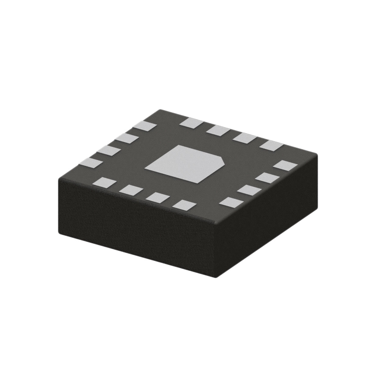
9FGV1006CQ506LTGI8
Search Product
Search Post
— IC芯片 | 连接器 | 传感器 | 被动器件 —
Search productSearch post
— IC芯片 | 连接器 | 传感器 | 被动器件 —
Consult the customer manager about the wholesale price.
consultation hotline:86-132-6715-2157
email:[email protected]
Contact the product manager for consultation. One-stop consultation is available.
Do you want a lower wholesale price? Please send us your inquiry and we will reply immediately.
The 9FGV1006CQ506LTGI8 is a PhiClock programmable clock generator manufactured by Renesas Electronics. It features one circuit with a 1:6 input-to-output ratio, supporting differential outputs. The device operates within a supply voltage range of 1.71V to 3.465V and supports maximum frequencies of 200MHz and 325MHz. It utilizes HCSL, LVCMOS, LVDS, or crystal inputs to generate CML, HCSL, LP-HCSL, LVCMOS, LVDS, or LVPECL outputs. The component is housed in a 16-TFLGA package with an exposed pad and functions reliably across a temperature range of -40°C to 85°C.
Verify the specific suffix LTGI8 for tape-and-reel packaging configuration. Confirm current availability status as some variants in this series have been marked as obsolete or discontinued by the manufacturer. Ensure compliance with RoHS3 specifications and MSL level 3 handling requirements during assembly.
Select this model when a 1:6 clock division ratio is required with support for both single-ended and differential outputs. Verify that the target system voltage aligns with the 1.71V to 3.465V operating range. Consider the 16-TFLGA package dimensions if board space is constrained compared to larger QFN packages.
This component belongs to the 9FGV1006 series within Renesas' PhiClock portfolio. It shares architectural similarities with other members like the 9FGV1002 and 9FGV1004 but is distinguished by its specific pin count and output configuration capabilities designed for complex multi-clock domain applications.
Publicly confirmed substitute part numbers are not available in the provided documentation. Users should consult official Renesas obsolescence notices for potential lifecycle management strategies.
 9FGV1006CQ506LTGI8
The activity of extra discounts on wholesale prices is in full swing…
Please fill in your contact information and we will send you the latest wholesale price list.