ChipApex | Global Electronic Components Supplier
9FGV1008B200LTGI
Search Product
Search Post
— IC芯片 | 连接器 | 传感器 | 被动器件 —
Search productSearch post
— IC芯片 | 连接器 | 传感器 | 被动器件 —
Consult the customer manager about the wholesale price.
consultation hotline:86-132-6715-2157
email:[email protected]
Contact the product manager for consultation. One-stop consultation is available.
Do you want a lower wholesale price? Please send us your inquiry and we will reply immediately.
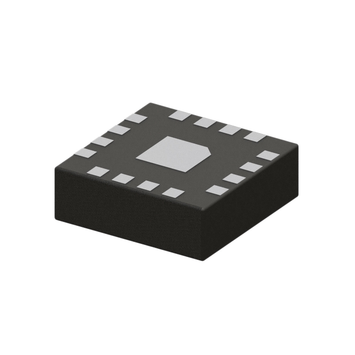
The 9FGV1008B200LTGI is a programmable clock generator from the Renesas PhiClock family, designed for high-performance data communication applications. It features an LP-HCSL and LVDS output interface with a maximum frequency of 400 MHz. The device operates on a single supply voltage ranging from 3.135 V to 3.465 V and supports a crystal input frequency of 50 MHz. Packaged in a 24-lead LGA (4.0 x 4.0 mm) format, it functions within a temperature range of -40°C to 85°C. Key electrical parameters include a typical power consumption of 100 mW and compliance with PCIe Gen1 through Gen4 jitter specifications.
Verify the exact suffix 'B200' against official Renesas documentation to confirm factory configuration settings, as this series consists of factory-configurable devices. Ensure compatibility with the required I²C address and OTP configuration defaults if software selection is utilized. Confirm package dimensions match the LTG24 specification (4.0 x 4.0 x 1.4 mm) during mechanical design review.
Select this component when both LP-HCSL and LVDS outputs are required simultaneously for mixed-signal environments. Verify that the 50 MHz crystal input matches the system oscillator availability. Consider the 24-lead LGA package constraints for PCB layout, ensuring adequate thermal relief and solder mask definitions for the 0.5 mm pitch leads.
This part belongs to the 9FGV1001C-9FGV1008C PhiClock™ family, which offers programmable clock generation with multiple output configurations. Unlike fixed-function generators, these devices allow customization of output frequencies and types at the factory, providing flexibility for various high-speed serial link applications without redesigning the clock tree.
Direct substitutes within the same family include 9FGV1004CQ501LTGI8 and 9FGV1006C000LTGI, provided the output count and signal types (LP-HCSL/LVDS) align with the design requirements. Cross-referencing must verify identical pinout and electrical characteristics, particularly regarding supply voltage ranges and jitter performance metrics.
 9FGV1008B200LTGI
The activity of extra discounts on wholesale prices is in full swing…
Please fill in your contact information and we will send you the latest wholesale price list.