ChipApex | Global Electronic Components Supplier
9FGV1008B201LTGI8
Search Product
Search Post
— IC芯片 | 连接器 | 传感器 | 被动器件 —
Search productSearch post
— IC芯片 | 连接器 | 传感器 | 被动器件 —
Consult the customer manager about the wholesale price.
consultation hotline:86-132-6715-2157
email:[email protected]
Contact the product manager for consultation. One-stop consultation is available.
Do you want a lower wholesale price? Please send us your inquiry and we will reply immediately.
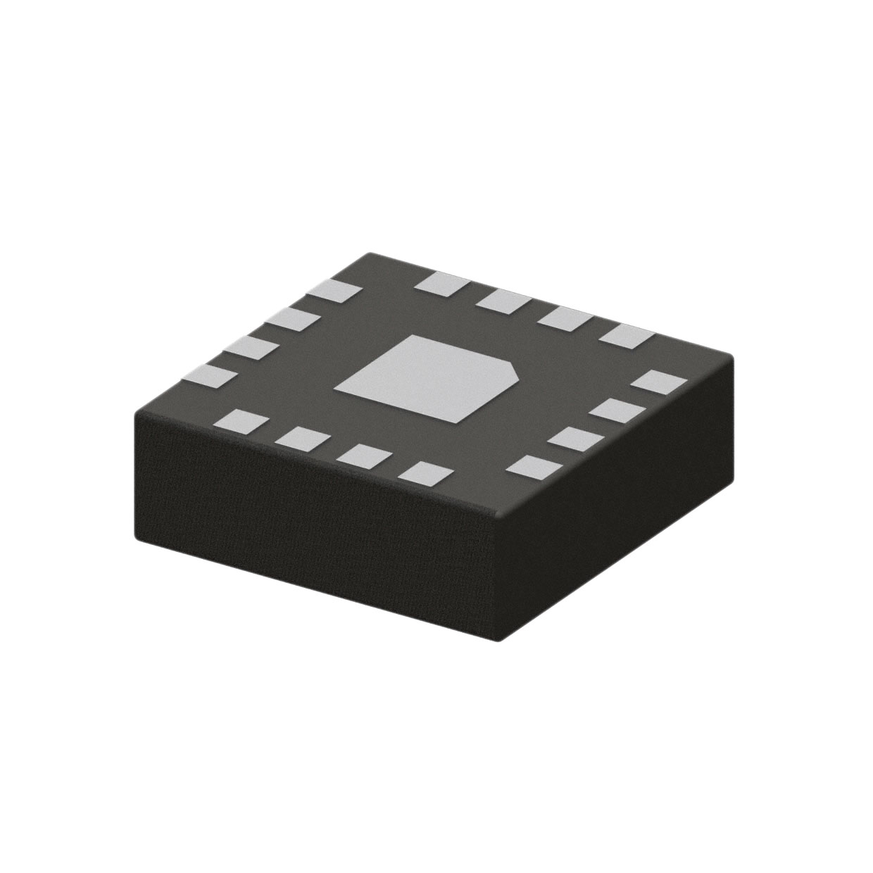
The 9FGV1008B201LTGI8 is a programmable clock generator from Renesas' PhiClock family, designed for high-speed interface timing. It features an integrated PLL and supports multiple input types including crystals, LVCMOS, LVDS, and HCSL. The device provides six differential outputs capable of LP-HCSL and LVDS signaling formats. It operates within a supply voltage range of 1.71V to 3.465V across three domains and functions reliably in temperatures from -40°C to 85°C. The component is housed in a 24-lead TFLGA package with an exposed pad.
Verify the specific suffix B201LTGI8 against the official 9FGV100xC datasheet addendum to confirm factory-configured frequency parameters. Confirm availability status as distribution channels may report obsolete or limited stock for specific programming variants. Ensure ESD handling protocols are followed during procurement and storage.
Select this model when six synchronized differential outputs are required for PCIe or SATA topologies. Verify that the fixed output frequencies match the target interface specifications, as this variant is factory-programmed. Compare power consumption requirements against the 1.8V and 3.3V operating modes to optimize system efficiency.
This component belongs to the 9FGV100xC series, which includes models like the 9FGV1002C and 9FGV1004C. These devices share the PhiClock architecture but differ in output counts and pinout configurations. The 9FGV1008 variant specifically targets designs requiring higher fan-out capabilities compared to the 9FGV1002 series.
Direct replacements include other 9FGV100xC family members such as the 9FGV1004C or 9FGV1006C if output count and pin compatibility allow. Verify that substitute parts support the same LP-HCSL and LVDS output standards and meet the required jitter performance for the specific application.
 9FGV1008B201LTGI8
The activity of extra discounts on wholesale prices is in full swing…
Please fill in your contact information and we will send you the latest wholesale price list.