 ChipApex | Global Electronic Components Supplier

SEARCH
Search Product
Search Post
— IC芯片 | 连接器 | 传感器 | 被动器件 —
Search productSearch post
— IC芯片 | 连接器 | 传感器 | 被动器件 —
Consult the customer manager about the wholesale price.
consultation hotline:86-132-6715-2157
email:[email protected]
Contact the product manager for consultation. One-stop consultation is available.
Do you want a lower wholesale price? Please send us your inquiry and we will reply immediately.
9SBV0802AKILFT is listed in the Clock Buffers, Drivers range at ChipApex. The manufacturer field lists Renesas Electronics Corporation. Its product description is 9SBV0802A DUAL 1:4 1V SINGLE END. Review the specifications below when checking this part for your BOM.
The Renesas 9SBV0802AKILFT is a dual fanout buffer designed for low-power clock distribution. It features two independent circuits, each providing a 1:4 single-ended output ratio from an LVCMOS input to LVCMOS outputs. The device operates within a supply voltage range of 1.7V to 1.9V and supports maximum frequencies up to 48 MHz. Packaged in a 20-VFQFN exposed pad (4x4 mm) suitable for surface mount assembly, it functions reliably across an extended industrial temperature range of -40°C to 85°C.
Verify the package type matches Tape & Reel or Cut Tape formats as specified. Confirm the 20-VFQFN footprint dimensions align with PCB layout requirements. Ensure the 1.7V-1.9V supply rail is stable for proper logic level translation. Check for RoHS compliance documentation if required by manufacturing standards.
Select this component when dual-channel single-ended buffering is required for LVCMOS signals. The 48 MHz limit suits lower-speed clocking needs compared to high-frequency PLL generators. The 20-VFQFN package offers a compact solution for space-constrained designs. Verify that the 1.9V max supply voltage fits the target system power budget.
This part belongs to the 9SBV0802 series of clock buffers. It serves as a distribution element for converting one input signal into four buffered outputs. The device complements clock generators by managing signal integrity and load driving capabilities in multi-drop clock networks.
Public confirmed substitute part numbers are not available in the provided source material.
Explore related parts through Clock/Timing, Integrated Circuits (ICs), all product categories, ChipApex homepage.
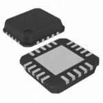 9SBV0802AKILFT

The activity of extra discounts on wholesale prices is in full swing…
Please fill in your contact information and we will send you the latest wholesale price list.




