 ChipApex | Global Electronic Components Supplier

SEARCH
Search Product
Search Post
— IC芯片 | 连接器 | 传感器 | 被动器件 —
Search productSearch post
— IC芯片 | 连接器 | 传感器 | 被动器件 —
Consult the customer manager about the wholesale price.
consultation hotline:86-132-6715-2157
email:[email protected]
Contact the product manager for consultation. One-stop consultation is available.
Do you want a lower wholesale price? Please send us your inquiry and we will reply immediately.
A1010B-2PLG44C is listed in the Field Programmable Gate Array range at ChipApex. The manufacturer field lists Microsemi Corporation. Its product description is IC FPGA 34 I/O 44PLCC. Review the specifications below when checking this part for your BOM.
The A1010B-2PLG44C is a Field Programmable Gate Array from the ACT 1 Series, manufactured by Microsemi Corporation. It features 1200 gate array equivalent gates and 295 programmable logic modules. The device supports up to 34 user I/Os and includes a maximum of 147 flip-flops. It utilizes PLICE antifuse technology on a 1.0 micron CMOS process. The component operates within a commercial temperature range of 0°C to +70°C. It is housed in a 44-pin Plastic J-Leaded Chip Carrier package. The standard speed grade provides a maximum data rate of 75 MHz at 5V.
Verify the specific ordering suffixes against the manufacturer's current product plan to confirm availability. Ensure the package type matches the required pin count and form factor. Check for any end-of-life notifications or obsolescence warnings associated with this legacy component series before finalizing procurement decisions.
Select this device when a small-scale FPGA with nonvolatile configuration is required. Consider the 44-pin package constraint for board space. Evaluate the 1200 gate capacity against design complexity. Verify that the 5V operating voltage aligns with system power rails. Confirm that the commercial temperature range meets environmental requirements.
This component belongs to the ACT 1 Series of FPGAs, which were among the first commercially available field-programmable gate arrays. The series is characterized by its use of antifuse technology rather than volatile SRAM or flash configurations. It represents an early generation of reprogrammable logic devices designed for rapid prototyping and low-volume production applications.
Direct replacements are limited due to the proprietary PLICE antifuse architecture. Review Actel/Microsemi successor families such as the ProASIC or SmartFusion series for modern equivalents. Verify pin compatibility and logic resource scaling when migrating to newer technologies.
The PRA and PRB pins serve as independent diagnostic probe outputs. They allow users to observe any two internal signals in real-time during debugging. These pins can also function as standard user-defined I/Os after debugging is complete.
The device uses Actel’s patented PLICE antifuse technology. Programming involves blowing specific antifuses to create permanent connections between logic modules and routing tracks. This process retains the programmed design without requiring external memory or power.
For the standard speed grade, the maximum data rate is 75 MHz when operating at 5V. The maximum clock frequency for flip-flops is specified as 70 MHz under worst-case commercial conditions.
Explore related parts through Embedded, Integrated Circuits (ICs), all product categories, ChipApex homepage.


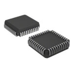 A1010B-2PLG44C

The activity of extra discounts on wholesale prices is in full swing…
Please fill in your contact information and we will send you the latest wholesale price list.



