 ChipApex | Global Electronic Components Supplier

SEARCH
Search Product
Search Post
— IC芯片 | 连接器 | 传感器 | 被动器件 —
Search productSearch post
— IC芯片 | 连接器 | 传感器 | 被动器件 —
Consult the customer manager about the wholesale price.
consultation hotline:86-132-6715-2157
email:[email protected]
Contact the product manager for consultation. One-stop consultation is available.
Do you want a lower wholesale price? Please send us your inquiry and we will reply immediately.
A1010B-2PLG44I is listed in the Field Programmable Gate Array range at ChipApex. The manufacturer field lists Microsemi Corporation. Its product description is IC FPGA 34 I/O 44PLCC. Review the specifications below when checking this part for your BOM.
The A1010B-2PLG44I is a Field Programmable Gate Array from the ACT 1 Series, manufactured by Microsemi Corporation. It features 295 logic modules and 1200 gate array equivalent gates. The device utilizes PLICE antifuse technology for nonvolatile user programming. It operates within an industrial temperature range of -40°C to +85°C and supports a maximum data rate of 75 MHz at 5V. The component is housed in a 44-pin Plastic J-Leaded Chip Carrier package with 34 user I/Os.
Verify the specific ordering suffix 'I' confirms the industrial temperature rating (-40°C to +85°C) as defined in the ACT 1 datasheet. Confirm the package type matches the 44-pin plastic leaded chip carrier specification. Check for current availability status as older Actel/Microsemi components may be discontinued or subject to last-time buys.
Select this model when 295 logic modules are sufficient for the design complexity. Ensure the application requires the industrial temperature grade rather than commercial or military options. Verify that the 44-pin package footprint fits the PCB layout constraints compared to other available pin counts like 68 or 84.
This component belongs to the ACT 1 family of FPGAs, which uses 1.0 micron CMOS technology. The family includes variants like A1020B with higher capacity. The 'A1010' designation indicates the 1200-gate density level within the series.
Direct replacements include other ACT 1 devices such as A1010B-1PLG44I or A1010B-3PLG44I for different speed grades. Cross-family migration to Microsemi SmartFusion or IGLOO may require significant architectural redesign.
The MODE pin controls multifunction pins (DCLK, PRA, PRB, SDI). When HIGH, special functions are active; when LOW, they function as standard I/O.
It offers tight fanout delay distributions by limiting interconnect paths to a maximum of four antifuses, ensuring predictable performance through automatic place and route.
Yes, the Probe A and Probe B pins can function as user-defined I/Os once debugging is completed.
Explore related parts through Embedded, Integrated Circuits (ICs), all product categories, ChipApex homepage.
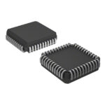 A1010B-2PLG44I

The activity of extra discounts on wholesale prices is in full swing…
Please fill in your contact information and we will send you the latest wholesale price list.






