 ChipApex | Global Electronic Components Supplier

SEARCH
Search Product
Search Post
— IC芯片 | 连接器 | 传感器 | 被动器件 —
Search productSearch post
— IC芯片 | 连接器 | 传感器 | 被动器件 —
Consult the customer manager about the wholesale price.
consultation hotline:86-132-6715-2157
email:[email protected]
Contact the product manager for consultation. One-stop consultation is available.
Do you want a lower wholesale price? Please send us your inquiry and we will reply immediately.
A14V25A-VQG100C is listed in the Field Programmable Gate Array range at ChipApex. The manufacturer field lists Microsemi Corporation. Its product description is IC FPGA 83 I/O 100VQFP. Review the specifications below when checking this part for your BOM.
The A14V25A-VQG100C is a Field Programmable Gate Array (FPGA) from the Microsemi ACT V series. It features 375 Configurable Logic Blocks (CLBs) and approximately 25,000 equivalent gates. The device operates on a single 3.3V supply voltage and supports up to 96 user-programmable I/O pins. It is housed in a 100-pin Very Thin Quad Flat Package (VQFP) with a 1 mm height. The component is rated for commercial temperature operation ranging from 0°C to 70°C.
Verify the specific suffix 'C' confirms the commercial temperature range of 0°C to 70°C against the official datasheet. Confirm the package designation matches the 100-pin VQFP physical dimensions. Ensure compatibility with 3.3V I/O standards if interfacing with modern logic families. Check for any RoHS compliance documentation required by the end application.
Select this model when 375 CLBs are sufficient for the design complexity. Verify that the 100-pin VQFP footprint fits the PCB layout constraints. Compare performance metrics such as clock-to-output delay against system timing requirements. Consider the ACT V family's place-and-route predictability for reliable timing closure.
This part belongs to the ACT V family, which succeeded the ACT III series. It offers increased logic density compared to the A14V15A while maintaining similar pin counts. The ACT V series was designed to bridge the gap between low-density PLDs and larger FPGAs, offering a balance of speed and resource availability.
Direct replacements may include other ACT V variants like the A14V35A if higher logic density is acceptable. Cross-family migration to SmartFusion or IGLOO requires significant architectural redesign. Verify pinout compatibility before substituting with older ACT III parts.
Explore related parts through Embedded, Integrated Circuits (ICs), all product categories, ChipApex homepage.


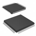 A14V25A-VQG100C

The activity of extra discounts on wholesale prices is in full swing…
Please fill in your contact information and we will send you the latest wholesale price list.



