 ChipApex | Global Electronic Components Supplier

SEARCH
Search Product
Search Post
— IC芯片 | 连接器 | 传感器 | 被动器件 —
Search productSearch post
— IC芯片 | 连接器 | 传感器 | 被动器件 —
Consult the customer manager about the wholesale price.
consultation hotline:86-132-6715-2157
email:[email protected]
Contact the product manager for consultation. One-stop consultation is available.
Do you want a lower wholesale price? Please send us your inquiry and we will reply immediately.
A3P1000-FGG144T is listed in the Field Programmable Gate Array range at ChipApex. The manufacturer field lists Microchip Technology. Its product description is IC FPGA 97 I/O 144FBGA. Review the specifications below when checking this part for your BOM.
The A3P1000-FGG144T is a ProASIC3 Flash Field Programmable Gate Array manufactured by Microchip Technology. It features 1,000,000 system gates and 24,576 Configurable Logic Blocks (CLBs). The device supports up to 144 kbits of True Dual-Port SRAM and provides 97 user I/Os. It operates within a supply voltage range of 1.425 V to 1.575 V at a nominal 1.5 V. The component is housed in a 144-pin FBGA package with a 1 mm pitch. It supports maximum operating frequencies up to 350 MHz and functions within an industrial temperature range of 0°C to +85°C.
Verify the suffix 'T' indicates tape-and-reel packaging when sourcing components. Confirm RoHS compliance status as older revisions may differ. Ensure ESD handling protocols are followed due to moisture sensitivity classification. Cross-reference the specific date code against manufacturer obsolescence notices to guarantee long-term availability for production runs.
Select this model for designs requiring 1 million system gates within a compact 144-pin footprint. Compare against the A3P1000-FG144 variant if tray packaging is preferred over reel packaging. Evaluate power consumption requirements against the 1.5 V core voltage specifications. Consider the A3P250 series if lower gate counts suffice for reduced cost and pin count.
This component belongs to the Microchip ProASIC3 Flash family, which bridges the gap between ASICs and traditional SRAM-based FPGAs. The family emphasizes low power consumption and immediate operational readiness. The A3P1000 represents the high-density tier within the 144-pin package options, offering significant logic capacity for complex embedded applications.
The A3P1000-FG144 serves as a pin-compatible alternative differing primarily in packaging format. Verify that any substitute maintains the same 1.5 V core voltage and I/O bank configurations. Check for updated software toolchain compatibility with newer FPGA design suites.
Explore related parts through Embedded, Integrated Circuits (ICs), all product categories, ChipApex homepage.


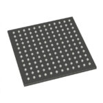 A3P1000-FGG144T

The activity of extra discounts on wholesale prices is in full swing…
Please fill in your contact information and we will send you the latest wholesale price list.



