 ChipApex | Global Electronic Components Supplier

SEARCH
Search Product
Search Post
— IC芯片 | 连接器 | 传感器 | 被动器件 —
Search productSearch post
— IC芯片 | 连接器 | 传感器 | 被动器件 —
Consult the customer manager about the wholesale price.
consultation hotline:86-132-6715-2157
email:[email protected]
Contact the product manager for consultation. One-stop consultation is available.
Do you want a lower wholesale price? Please send us your inquiry and we will reply immediately.
A3P250-2FGG144 is listed in the Field Programmable Gate Array range at ChipApex. The manufacturer field lists Microchip Technology. Its product description is IC FPGA 97 I/O 144FBGA. Review the specifications below when checking this part for your BOM.
The A3P250-2FGG144 is a ProASIC3 Flash Field Programmable Gate Array manufactured by Microchip Technology. It features 250,000 system gates and 6,144 configurable logic blocks (CLBs). The device supports a maximum operating frequency of 310 MHz and includes 36 kbits of embedded SRAM. It provides 97 user I/Os and operates within a supply voltage range of 1.425 V to 1.575 V. The component is housed in a 144-pin Fine-Pitch Ball Grid Array (FPBGA) package with a 13x13 mm footprint. It supports mixed-voltage operation for 1.5 V, 1.8 V, 2.5 V, and 3.3 V banks.
Verify the specific speed grade suffix '2' against the manufacturer's datasheet to confirm the 310 MHz performance rating. Ensure the FPBGA-144 package dimensions match the target PCB layout requirements. Confirm RoHS compliance status through official Microchip documentation prior to procurement.
Select this model when a balance of moderate logic capacity and high-speed performance is required. Compare against the A3P250-1FGG144 if lower speed grades suffice for cost reduction. Consider the M1A3P250 variant if integrated ARM Cortex-M1 processing capabilities are necessary for the application.
This component belongs to the ProASIC3 Flash FPGA family, which bridges the gap between ASICs and standard FPGAs. It utilizes a 130-nm process technology. The family is characterized by its reprogrammable flash nature, offering design flexibility with the persistence of ASIC-like power efficiency and immediate operational readiness.
The A3P250-1FGG144 serves as a verified lower-speed substitute within the same package. For pin-compatible upgrades or downgrades, verify that the timing constraints of the design accommodate the specific speed bin differences between the -1 and -2 variants.
Explore related parts through Embedded, Integrated Circuits (ICs), all product categories, ChipApex homepage.


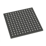 A3P250-2FGG144

The activity of extra discounts on wholesale prices is in full swing…
Please fill in your contact information and we will send you the latest wholesale price list.



