 ChipApex | Global Electronic Components Supplier

SEARCH
Search Product
Search Post
— IC芯片 | 连接器 | 传感器 | 被动器件 —
Search productSearch post
— IC芯片 | 连接器 | 传感器 | 被动器件 —
Consult the customer manager about the wholesale price.
consultation hotline:86-132-6715-2157
email:[email protected]
Contact the product manager for consultation. One-stop consultation is available.
Do you want a lower wholesale price? Please send us your inquiry and we will reply immediately.
A3P250L-1FGG144 is listed in the Field Programmable Gate Array range at ChipApex. The manufacturer field lists Microsemi Corporation. Its product description is IC FPGA 97 I/O 144FBGA. Review the specifications below when checking this part for your BOM.
The A3P250L-1FGG144 is a Field Programmable Gate Array (FPGA) belonging to the ProASIC3L Flash family manufactured by Microsemi. It features 250,000 system gates and 6,144 configurable logic blocks (CLBs). The device supports a maximum clock frequency of 350 MHz and includes up to 144 kbits of True Dual-Port SRAM. It utilizes a 144-pin Low Profile Ball Grid Array (LBGA) package with 97 user I/Os. Operating voltage ranges from 1.14 V to 1.575 V, with an industrial temperature range of -40 °C to 85 °C.
Verify the specific suffix '1' indicates the industrial temperature grade (-40°C to +85°C) and speed bin. Confirm RoHS compliance status as manufacturing processes may evolve. Check for active production status or last-time buy notifications due to the mature nature of the ProASIC3L series.
Select this model when non-volatile configuration and high reliability are required. Compare against the standard A3P250 if commercial temperature range suffices. Ensure the 144-pin LBGA footprint fits the PCB layout constraints compared to QFP alternatives.
This component is part of the ProASIC3L series, which offers lower power consumption than the standard ProASIC3 family while maintaining similar gate densities. It bridges the gap between ASICs and complex FPGAs, offering reprogrammability with flash persistence.
Direct pin-compatible replacements within the same package include other speed grades of the A3P250L series. Cross-family migration to ProASIC3 Plus or SmartFusion2 requires schematic redesign due to architectural differences.
Explore related parts through Embedded, Integrated Circuits (ICs), all product categories, ChipApex homepage.
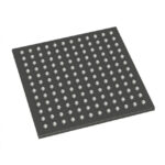 A3P250L-1FGG144

The activity of extra discounts on wholesale prices is in full swing…
Please fill in your contact information and we will send you the latest wholesale price list.





