 ChipApex | Global Electronic Components Supplier

SEARCH
Search Product
Search Post
— IC芯片 | 连接器 | 传感器 | 被动器件 —
Search productSearch post
— IC芯片 | 连接器 | 传感器 | 被动器件 —
Consult the customer manager about the wholesale price.
consultation hotline:86-132-6715-2157
email:[email protected]
Contact the product manager for consultation. One-stop consultation is available.
Do you want a lower wholesale price? Please send us your inquiry and we will reply immediately.
A3P400-1FG256 is listed in the Field Programmable Gate Array range at ChipApex. The manufacturer field lists Microchip Technology. Its product description is IC FPGA 178 I/O 256FBGA. Review the specifications below when checking this part for your BOM.
The A3P400-1FG256 is a ProASIC3 Flash Field Programmable Gate Array manufactured by Microchip Technology. It features 400,000 system gates and supports up to 178 user I/Os within a 256-pin FBGA package. The device operates on a core voltage ranging from 1.425 V to 1.575 V and supports mixed-voltage I/O standards including 1.5 V, 1.8 V, 2.5 V, and 3.3 V. It offers a maximum operating frequency of 310 MHz and includes embedded SRAM for configuration storage. The component is designed for surface-mount installation and functions across an industrial temperature range.
Verify the specific suffix designation against official Microchip documentation, as variations such as -1 or -2 indicate different speed grades. Confirm RoHS compliance status directly with the manufacturer, as historical batches may differ. Ensure the ordering quantity aligns with standard factory packaging requirements to avoid handling fees. Request current production lifecycle status to confirm availability for long-term deployment.
Select this model when instant-on capability is critical to eliminate external configuration EEPROMs. Compare gate density and I/O count against higher-tier ProASIC3 variants if additional logic resources are required. Verify that the 256-pin FBGA footprint matches the target PCB layout constraints. Ensure the design accommodates the specific power supply sequencing required for the 1.5 V core and selected I/O voltages.
This component belongs to the Microchip ProASIC3 family, which bridges the gap between ASICs and traditional FPGAs by offering flash-based non-volatility. The A3P400 variant provides mid-range capacity suitable for complex digital logic applications. It serves as a pin-compatible alternative to previous Actel FPGA generations, maintaining software compatibility while enhancing performance and reducing power consumption.
Direct pin-compatible substitutes within the same package include other members of the A3P300, A3P600, or M1A3P400 series, provided logic resource requirements are met. Cross-family replacements from Actel or Lattice may require significant schematic and layout modifications due to architectural differences.
Explore related parts through Embedded, Integrated Circuits (ICs), all product categories, ChipApex homepage.


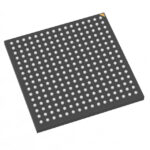 A3P400-1FG256

The activity of extra discounts on wholesale prices is in full swing…
Please fill in your contact information and we will send you the latest wholesale price list.




