 ChipApex | Global Electronic Components Supplier

SEARCH
Search Product
Search Post
— IC芯片 | 连接器 | 传感器 | 被动器件 —
Search productSearch post
— IC芯片 | 连接器 | 传感器 | 被动器件 —
Consult the customer manager about the wholesale price.
consultation hotline:86-132-6715-2157
email:[email protected]
Contact the product manager for consultation. One-stop consultation is available.
Do you want a lower wholesale price? Please send us your inquiry and we will reply immediately.
A3P400-2FG484 is listed in the Field Programmable Gate Array range at ChipApex. The manufacturer field lists Microsemi Corporation. Its product description is IC FPGA 194 I/O 484FBGA. Review the specifications below when checking this part for your BOM.
The A3P400-2FG484 is a ProASIC3 Flash Field Programmable Gate Array manufactured by Microsemi. It features 400,000 system gates and 9,216 VersaTiles within a 484-pin Fine Pitch Ball Grid Array (FG484) package with a 1.0 mm pitch. The device operates at a maximum frequency of 350 MHz and supports up to 194 user I/Os across four banks. It includes 54 kbits of embedded SRAM and 1 kbit of nonvolatile FlashROM. The -2 speed grade indicates performance 25% faster than the standard grade, while the 'I' suffix denotes an industrial temperature range of -40°C to +100°C.
Verify the specific ordering suffixes against the manufacturer's official datasheet to confirm package type, speed grade, and temperature range. Ensure compatibility with existing board layouts as FG256 and FG484 packages are footprint-compatible. Confirm RoHS compliance status if required for your manufacturing process.
Select this device when high-density logic is needed with nonvolatile configuration storage. Consider the -2 speed grade for applications requiring higher clock frequencies than the standard grade provides. Verify that the 194 available I/Os meet interface requirements and check if the embedded memory sizes are sufficient for your design needs.
This component belongs to the ProASIC3 Flash family, which bridges the gap between ASICs and SRAM-based FPGAs. It offers reprogrammability with the security and instant-on benefits of flash technology. The A3P400 represents a mid-range density option within the family, suitable for complex logic designs without the cost of higher-density parts.
Check for pin-compatible alternatives within the same package size. Higher density devices like the A3P600 or A3P1000 may be compatible if resources allow. Lower density options like the A3P250 might fit if logic requirements are reduced. Always verify electrical characteristics and timing constraints before substitution.
No, the standard A3P400 does not support ARM Cortex-M1. Devices with ARM support have part numbers starting with M1A3P.
The -2 speed grade offers performance that is 25% faster than the standard (-1) grade, allowing for higher maximum operating frequencies.
No, the FlashROM can only be programmed via the JTAG programming interface and cannot be accessed or written by the internal FPGA logic.
Explore related parts through Embedded, Integrated Circuits (ICs), all product categories, ChipApex homepage.


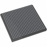 A3P400-2FG484

The activity of extra discounts on wholesale prices is in full swing…
Please fill in your contact information and we will send you the latest wholesale price list.



