 ChipApex | Global Electronic Components Supplier

SEARCH
Search Product
Search Post
— IC芯片 | 连接器 | 传感器 | 被动器件 —
Search productSearch post
— IC芯片 | 连接器 | 传感器 | 被动器件 —
Consult the customer manager about the wholesale price.
consultation hotline:86-132-6715-2157
email:[email protected]
Contact the product manager for consultation. One-stop consultation is available.
Do you want a lower wholesale price? Please send us your inquiry and we will reply immediately.
The A3PE600-PQ208I is a ProASIC3E flash-based Field Programmable Gate Array manufactured by Microsemi. It provides 600,000 system gates and 13,824 VersaTiles (D-flip-flops). The device includes 108 kbits of True Dual-Port SRAM organized into 24 blocks of 4,608 bits each. It features six Clock Conditioning Circuits (CCCs) with integrated PLLs and supports up to 147 user I/Os in the PQFP-208 package. The maximum operating frequency is 350 MHz. The 'I' suffix indicates an industrial temperature range of -40°C to +100°C junction temperature.
Verify the specific ordering suffix against the manufacturer's current datasheet revision to confirm package type and temperature grade. Ensure the component matches the required speed grade for the target application timing constraints. Check for RoHS compliance status if environmental regulations apply to the final assembly process.
Select this device when nonvolatile configuration and instant-on capability are required. The PQ208 package limits available CCCs to two PLLs; larger packages offer full clocking resources. Verify that the 147 user I/O count meets interface requirements. Consider the 130-nm process node for power consumption characteristics relative to newer technologies.
This component belongs to the ProASIC3E family, which succeeded the ProASIC PLUS series. It utilizes a 130-nm CMOS process with seven metal layers. The family offers a balance between ASIC unit costs and FPGA flexibility. It is designed for applications requiring high security and low power consumption in consumer, networking, and avionics markets.
Pin-compatible alternatives within the ProASIC3E family include higher-density devices such as the A3PE1500 and A3PE3000 in the same PQ208 package. Lower density options like the A3P600 from the standard ProASIC3 family may be considered if flash technology is not strictly required.
The PQ208 package supports only two PLLs, located at the center east and west sides, although all six CCC blocks remain usable for clock delay operations.
The 1 kbit FlashROM provides user-accessible nonvolatile storage for data such as IP addressing, calibration settings, serialization, and secure key storage.
No, the flash-based architecture stores configuration data on-chip, eliminating the need for external boot PROMs and enabling Instant On functionality.
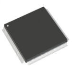 A3PE600-PQ208I

The activity of extra discounts on wholesale prices is in full swing…
Please fill in your contact information and we will send you the latest wholesale price list.






