 ChipApex | Global Electronic Components Supplier

SEARCH
Search Product
Search Post
— IC芯片 | 连接器 | 传感器 | 被动器件 —
Search productSearch post
— IC芯片 | 连接器 | 传感器 | 被动器件 —
Consult the customer manager about the wholesale price.
consultation hotline:86-132-6715-2157
email:[email protected]
Contact the product manager for consultation. One-stop consultation is available.
Do you want a lower wholesale price? Please send us your inquiry and we will reply immediately.
A3PN010-QNG48I is listed in the Field Programmable Gate Array range at ChipApex. The manufacturer field lists Microchip Technology. Its product description is IC FPGA 34 I/O 48QFN. Review the specifications below when checking this part for your BOM.
The A3PN010-QNG48I is a ProASIC3 nano field-programmable gate array (FPGA) manufactured by Microchip Technology. It features 260 logic elements and approximately 10,000 system gates within a 48-VFQFN package with exposed pad. The device supports 34 user I/Os and operates on a single 1.5V supply voltage ranging from 1.425V to 1.575V. It offers an industrial temperature range of -40°C to +100°C TJ and supports maximum data rates up to 700 Mbps for DDR interfaces.
Verify the specific suffix 'I' confirms the industrial temperature grade (-40°C to +100°C). Confirm the package type matches the 48-VFQFN footprint requirements. Check RoHS compliance status against current manufacturing notices. Ensure ESD handling procedures are followed during assembly due to moisture sensitivity level 3 classification.
Select this model when non-vatility and low pin count are required. Compare logic density against the AGLN010 series if lower power consumption is critical. Verify I/O voltage compatibility with connected peripherals before finalizing the design. Consider the 48-pin constraint for available signal routing.
This component belongs to the ProASIC3 nano family, designed for cost-sensitive applications needing small form factors. It bridges the gap between complex FPGAs and simple CPLDs. The family shares pin-out compatibility across different logic densities within the same package style.
Direct pin-compatible replacements within the ProASIC3 family include higher density variants like the A3P030-QNG48I, provided logic resources are sufficient. Lower density options may exist but require verification of functional equivalence. Cross-family migration to IGLOO nano requires schematic review due to architectural differences.
Explore related parts through Embedded, Integrated Circuits (ICs), all product categories, ChipApex homepage.


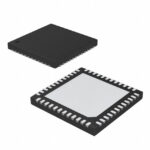 A3PN010-QNG48I

The activity of extra discounts on wholesale prices is in full swing…
Please fill in your contact information and we will send you the latest wholesale price list.



