 ChipApex | Global Electronic Components Supplier

SEARCH
Search Product
Search Post
— IC芯片 | 连接器 | 传感器 | 被动器件 —
Search productSearch post
— IC芯片 | 连接器 | 传感器 | 被动器件 —
Consult the customer manager about the wholesale price.
consultation hotline:86-132-6715-2157
email:[email protected]
Contact the product manager for consultation. One-stop consultation is available.
Do you want a lower wholesale price? Please send us your inquiry and we will reply immediately.
The A3PN250-Z1VQ100 is a ProASIC3 nano Flash Field Programmable Gate Array (FPGA) manufactured by Microchip Technology. It features 250,000 system gates and up to 36 kbits of True Dual-Port SRAM. The device supports up to 71 user I/Os with mixed-voltage operation capabilities for 1.5 V, 1.8 V, 2.5 V, and 3.3 V standards. It utilizes a 130-nm flash-based CMOS process, enabling instant-on functionality and non-volatile design retention. The FPGA operates at system frequencies up to 350 MHz and includes Clock Conditioning Circuits (CCC) with integrated PLLs. It is housed in a 100-pin VQFP package.
Verify the specific suffix 'Z1' against official Microchip documentation to confirm exact temperature range and package variant, as suffixes define environmental and mechanical specifications. Ensure compatibility with existing PCB footprints for the 100-VQFP package. Confirm moisture sensitivity level handling requirements during assembly. Validate that the selected revision aligns with current manufacturing notices and software tool support versions.
Select this component for designs requiring high gate density combined with non-vatile configuration and mixed-voltage I/O flexibility. Compare against standard ProASIC3 models if volatile configuration or lower power consumption is prioritized over instant-on capability. Evaluate the 36 kbit SRAM capacity against data buffering needs. Consider the 130-nm process node implications for future supply chain longevity compared to newer technology nodes.
This part belongs to the ProASIC3 nano family, which bridges the gap between low-density ASICs and complex FPGAs. The 'nano' designation indicates optimized power consumption and smaller form factors compared to the standard ProASIC3 line. It shares pin compatibility with other devices in the ProASIC3 family, facilitating scalable design transitions within the same package constraints.
A3PN250-VQG100: Pin-compatible alternative within the same family, verify voltage and temperature specs.
No, it uses reprogrammable Flash technology that retains the programmed design when powered off, eliminating the need for external configuration devices.
The device supports system performance up to 350 MHz.
Yes, it supports bank-selectable I/O voltages allowing simultaneous operation of 1.5 V, 1.8 V, 2.5 V, and 3.3 V standards across up to four banks.
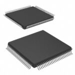 A3PN250-Z1VQ100

The activity of extra discounts on wholesale prices is in full swing…
Please fill in your contact information and we will send you the latest wholesale price list.






