 ChipApex | Global Electronic Components Supplier

SEARCH
Search Product
Search Post
— IC芯片 | 连接器 | 传感器 | 被动器件 —
Search productSearch post
— IC芯片 | 连接器 | 传感器 | 被动器件 —
Consult the customer manager about the wholesale price.
consultation hotline:86-132-6715-2157
email:[email protected]
Contact the product manager for consultation. One-stop consultation is available.
Do you want a lower wholesale price? Please send us your inquiry and we will reply immediately.
The A40MX02-1PL68M is a field-programmable gate array (FPGA) from the Microchip MX family, designed as a high-capacity single-chip ASIC alternative. It features 295 logic elements and approximately 3,000 system gates. The device supports mixed-voltage operation with supply voltage ranges of 4.5 V to 5.5 V or 3.0 V to 3.6 V. It provides 57 user-programmable I/O pins and utilizes a 68-pin PLCC package. The component operates within an industrial temperature range of -40°C to +85°C.
Verify the specific suffix 'M' against official Microchip documentation to confirm it denotes the industrial temperature grade (-40°C to +85°C). Ensure the ordering part number matches the exact package type and speed grade required for the design. Confirm RoHS compliance status through the manufacturer's current datasheet before procurement.
Select this model when a small FPGA footprint with mixed-voltage capability is required. The 68-pin PLCC package suits surface-mount designs needing moderate I/O density. Compare against the A40MX02-1PLG68I if commercial temperature range suffices, or consider higher gate counts in the A40MX series for more complex logic requirements.
This component belongs to the Actel/Microchip MX FPGA family, known for non-volatile flash-based technology. The A40MX02 variant represents the entry-level capacity within this series, offering a balance of logic resources and pin count for cost-sensitive applications requiring reprogrammability without external configuration memory.
Direct substitutes include other variants within the A40MX02 family such as the A40MX02-1PLG68I, provided the temperature grade and package match the application requirements. Cross-referencing speed grades and package types is essential when evaluating alternatives.


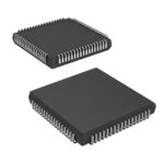 A40MX02-1PL68M

The activity of extra discounts on wholesale prices is in full swing…
Please fill in your contact information and we will send you the latest wholesale price list.



