 ChipApex | Global Electronic Components Supplier

SEARCH
Search Product
Search Post
— IC芯片 | 连接器 | 传感器 | 被动器件 —
Search productSearch post
— IC芯片 | 连接器 | 传感器 | 被动器件 —
Consult the customer manager about the wholesale price.
consultation hotline:86-132-6715-2157
email:[email protected]
Contact the product manager for consultation. One-stop consultation is available.
Do you want a lower wholesale price? Please send us your inquiry and we will reply immediately.
The A40MX02-3PL44 is a Field Programmable Gate Array (FPGA) from the Microchip MX series, designed as a high-capacity single-chip ASIC alternative. It features 295 Configurable Logic Blocks (CLBs) and approximately 3,000 system gates. The device supports mixed-voltage operation with core and I/O supplies of 3.3V or 5.0V. It is housed in a 44-pin PLCC package and operates within a commercial temperature range of 0°C to +70°C.
Verify the specific suffix against official datasheets to confirm package type and temperature grade. Ensure compatibility with existing design constraints regarding voltage levels and pin configurations before procurement.
Select this component for applications requiring moderate logic density with flexible voltage requirements. Consider the PLCC package form factor and commercial temperature range suitability for the target environment.
This part belongs to the A40MX family of SRAM-based FPGAs, offering non-volatile configuration memory options when paired with external flash. It serves as a bridge between complex CPLDs and larger FPGAs, providing flexibility for prototyping and low-to-medium volume production.
Direct substitutes include other variants within the A40MX series such as the A40MX02-3PL68 or A40MX04-3PLG44, depending on required I/O count and gate density. Verify pinout compatibility for direct replacements.
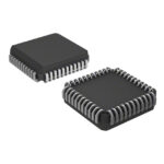 A40MX02-3PL44

The activity of extra discounts on wholesale prices is in full swing…
Please fill in your contact information and we will send you the latest wholesale price list.






