 ChipApex | Global Electronic Components Supplier

SEARCH
Search Product
Search Post
— IC芯片 | 连接器 | 传感器 | 被动器件 —
Search productSearch post
— IC芯片 | 连接器 | 传感器 | 被动器件 —
Consult the customer manager about the wholesale price.
consultation hotline:86-132-6715-2157
email:[email protected]
Contact the product manager for consultation. One-stop consultation is available.
Do you want a lower wholesale price? Please send us your inquiry and we will reply immediately.
The A40MX02-3VQ80 is a Field Programmable Gate Array (FPGA) from the Microchip Technology 40MX family. It features 295 Configurable Logic Blocks (CLBs) and approximately 3,000 system gates. The device supports mixed-voltage operation with core and I/O supplies of 5.0V or 3.3V. It utilizes SRAM-based non-volatile configuration technology and includes up to 2.5 kbits of configurable dual-port SRAM. The component is housed in an 80-pin VQFP package.
Verify the specific speed grade suffix against official Microchip documentation to ensure timing compliance. Confirm package availability as legacy FPGA families may have limited production runs. Check for RoHS compliance status and lead times directly with authorized distributors. Ensure ESD handling procedures are followed during storage and assembly due to the CMOS process technology.
Select this model when 3,000 system gates and 295 CLBs are sufficient for the target design. Choose the VQ80 package if space-constrained surface-mount assembly on an 80-pin footprint is required. Consider the 3.3V or 5.0V mixed-voltage capability if interfacing with legacy components. Verify that the SRAM-based configuration architecture aligns with the project's reprogrammability requirements.
This component belongs to the Actel 40MX family of SRAM-based FPGAs, originally developed by Actel Corporation before its acquisition by Microsemi and subsequently Microchip Technology. The 40MX series was designed to offer high-density logic in small packages, serving as a drop-in replacement for complex GALs and PLDs. The A40MX02 variant represents a specific gate count tier within this lineage.


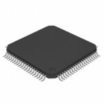 A40MX02-3VQ80

The activity of extra discounts on wholesale prices is in full swing…
Please fill in your contact information and we will send you the latest wholesale price list.



