 ChipApex | Global Electronic Components Supplier

SEARCH
Search Product
Search Post
— IC芯片 | 连接器 | 传感器 | 被动器件 —
Search productSearch post
— IC芯片 | 连接器 | 传感器 | 被动器件 —
Consult the customer manager about the wholesale price.
consultation hotline:86-132-6715-2157
email:[email protected]
Contact the product manager for consultation. One-stop consultation is available.
Do you want a lower wholesale price? Please send us your inquiry and we will reply immediately.
The A40MX02-PQG100A is a field-programmable gate array (FPGA) from the Microchip MX family, housed in a 100-pin PQFP package. It features approximately 3,000 system gates and 295 configurable logic blocks (CLBs). The device supports dual voltage operation at 3V to 3.6V and 4.75V to 5.25V. Key electrical parameters include a maximum clock frequency of 48.24 MHz and a CLB delay of 3.72 ns. It offers up to 2.5 kbits of configurable dual-port SRAM and supports up to 57 user-programmable I/O pins.
Verify the specific suffix against official Microchip documentation to confirm pinout compatibility and electrical characteristics. Ensure the source provides valid RoHS compliance data and moisture sensitivity level information before procurement. Cross-reference the part number with current distributor listings to confirm availability status.
Select this component when a moderate logic density around 3,000 gates is required within a 100-pin footprint. Consider the dual-voltage capability if the design requires flexibility between 3.3V and 5V systems. Evaluate the 48.24 MHz performance limit against the target application's timing requirements.
This part belongs to the A40MX series, which serves as a bridge between complex CPLDs and larger FPGAs. The MX family is known for its non-volatile flash technology, allowing instant-on functionality without external configuration memory. It targets applications needing reprogrammability with lower power consumption than traditional SRAM-based FPGAs.
Direct substitutes within the same package and logic density include the A40MX02-2PQG100 or A40MX02-FVQ100B. Verify that any replacement maintains the 100-pin PQFP form factor and compatible voltage ranges. Check for any pinout differences between variants in the A40MX02 lineup.


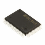 A40MX02-PQG100A

The activity of extra discounts on wholesale prices is in full swing…
Please fill in your contact information and we will send you the latest wholesale price list.




