 ChipApex | Global Electronic Components Supplier

SEARCH
Search Product
Search Post
— IC芯片 | 连接器 | 传感器 | 被动器件 —
Search productSearch post
— IC芯片 | 连接器 | 传感器 | 被动器件 —
Consult the customer manager about the wholesale price.
consultation hotline:86-132-6715-2157
email:[email protected]
Contact the product manager for consultation. One-stop consultation is available.
Do you want a lower wholesale price? Please send us your inquiry and we will reply immediately.
The A40MX04-1PL84 is a field-programmable gate array (FPGA) from the Microchip MX family, designed as a single-chip ASIC alternative. It features 6,000 system gates and 547 logic elements within a 68-pin PLCC package. The device operates on dual voltage supplies: 3V to 3.6V and 4.75V to 5.25V. It supports surface-mount installation with a commercial temperature range of 0°C to 70°C. Key specifications include 57 I/O pins, SRAM-based non-volatile configuration, and IEEE 1149.1 JTAG boundary scan support for testing.
Verify the specific suffix 'PL84' against official Microchip documentation, as standard datasheets typically list 'PLG68' or 'PLG84'. Confirm moisture sensitivity level 3 compliance and RoHS status during sourcing. Ensure the ordering part number matches the exact package and temperature grade required for your assembly process.
Select this component when a small form factor FPGA with fixed pin assignments is required. Compare against the A40MX02 for lower gate counts or the A42MX series for higher capacity. Verify that the 68-pin PLCC package fits the PCB footprint constraints and that the 57 available I/O pins meet the interface requirements.
This device belongs to the Actel MX family, acquired by Microchip Technology. The MX series is characterized by its fast wide-decode circuitry and low power consumption compared to traditional SRAM FPGAs. It serves as a bridge between discrete logic solutions and more complex programmable devices.
Publicly confirmed substitute part numbers are not available in the provided source material. Consult Microchip engineering for potential cross-references based on specific functional requirements.


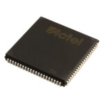 A40MX04-1PL84

The activity of extra discounts on wholesale prices is in full swing…
Please fill in your contact information and we will send you the latest wholesale price list.



