 ChipApex | Global Electronic Components Supplier

SEARCH
Search Product
Search Post
— IC芯片 | 连接器 | 传感器 | 被动器件 —
Search productSearch post
— IC芯片 | 连接器 | 传感器 | 被动器件 —
Consult the customer manager about the wholesale price.
consultation hotline:86-132-6715-2157
email:[email protected]
Contact the product manager for consultation. One-stop consultation is available.
Do you want a lower wholesale price? Please send us your inquiry and we will reply immediately.
The A40MX04-1PL84M is a field-programmable gate array (FPGA) from the Microchip MX family, designed as a high-capacity single-chip ASIC alternative. It features 6,000 system gates and 547 logic elements within a 68-pin PLCC package. The device operates on mixed-voltage supplies of 3V to 3.6V or 4.75V to 5.25V, supporting both core and I/O configurations. It includes up to 2.5 kbits of configurable dual-port SRAM and supports IEEE 1149.1 JTAG boundary scan testing for verification.
Verify the specific suffix 'M' against official Microchip documentation to confirm it denotes military temperature range or specific qualification standards, as standard commercial variants typically lack this designation. Confirm RoHS compliance status and moisture sensitivity level (MSL 3) prior to procurement. Ensure the source document explicitly validates the 'M' suffix functionality to avoid substitution errors.
Select this component when 6,000 system gates and 57 user-programmable I/O pins are required in a surface-mount PLCC package. Consider the MX family architecture for synthesis-friendly design methodologies and fast wide-decode circuitry. Evaluate the mixed-voltage supply requirements against the target system's power rails before finalizing the selection.
This part belongs to the A40MX04 series within the broader 40MX and 42MX FPGA families. These devices are positioned as high-capacity programmable logic solutions offering performance comparable to ASICs. The family supports various package options including PLCC, QFP, and BGA, catering to diverse integration needs across commercial and industrial sectors.
Publicly confirmed substitute part numbers for the A40MX04-1PL84M are not available in the provided reference data. Verify cross-references through official Microchip engineering change notices or authorized distributor databases before considering alternative components.


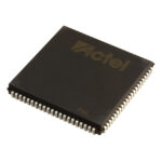 A40MX04-1PL84M

The activity of extra discounts on wholesale prices is in full swing…
Please fill in your contact information and we will send you the latest wholesale price list.



