 ChipApex | Global Electronic Components Supplier

SEARCH
Search Product
Search Post
— IC芯片 | 连接器 | 传感器 | 被动器件 —
Search productSearch post
— IC芯片 | 连接器 | 传感器 | 被动器件 —
Consult the customer manager about the wholesale price.
consultation hotline:86-132-6715-2157
email:[email protected]
Contact the product manager for consultation. One-stop consultation is available.
Do you want a lower wholesale price? Please send us your inquiry and we will reply immediately.
The A40MX04-2PL84I is a Field Programmable Gate Array (FPGA) from the Microchip MX family, featuring 6,000 system gates and 547 logic elements. It provides 69 user-programmable I/O pins within a PLCC-84 surface-mount package. The device operates on dual voltage supplies: 3.3V for the core and 5.0V for I/Os, with a supply range of 4.5V to 5.5V. It supports an industrial temperature range of -40°C to +85°C and includes IEEE 1149.1 JTAG boundary scan capabilities.
Verify the specific suffix 'I' confirms the industrial temperature grade (-40°C to +85°C) against the official datasheet. Confirm the PLCC-84 package type matches the target footprint. Check for recent Product Change Notifications regarding assembly sites or material composition updates before finalizing procurement orders.
Select this model when 6,000 system gates and 69 I/Os are required for mixed-voltage 3.3V/5.0V designs. Ensure the design utilizes the MX family's synthesis-friendly architecture. Compare against the A40MX04-2PQG100I if a PQFP-100 package is preferred over PLCC-84 for the same logical capacity.
This component belongs to the A40MX04 series within the broader MX FPGA portfolio. It shares the same 6,000-gate logical fabric as other variants like the A40MX04-2PLG44 but differs in package density and I/O count. The part represents a mid-range solution in the Actel/Microchip programmable logic lineup.
Direct functional substitutes include other A40MX04 variants such as A40MX04-2PLG84I or A40MX04-2PQG100I, provided the package footprint difference is accommodated by the PCB design. No cross-family replacements are officially confirmed without redesign.
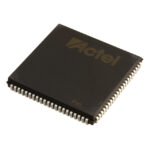 A40MX04-2PL84I

The activity of extra discounts on wholesale prices is in full swing…
Please fill in your contact information and we will send you the latest wholesale price list.





