 ChipApex | Global Electronic Components Supplier

SEARCH
Search Product
Search Post
— IC芯片 | 连接器 | 传感器 | 被动器件 —
Search productSearch post
— IC芯片 | 连接器 | 传感器 | 被动器件 —
Consult the customer manager about the wholesale price.
consultation hotline:86-132-6715-2157
email:[email protected]
Contact the product manager for consultation. One-stop consultation is available.
Do you want a lower wholesale price? Please send us your inquiry and we will reply immediately.
The A40MX04-2PLG68 is a Field Programmable Gate Array (FPGA) from the Microchip MX family, manufactured by Microchip Technology. It features 547 Logic Elements and approximately 6,000 system gates within a 68-pin PLCC package. The device supports mixed-voltage operation with supply voltages of 3.3 V or 5 V. It operates within an industrial temperature range of -40°C to +85°C and includes 57 user-programmable I/O pins. The component utilizes flash-based non-volatile memory technology for configuration.
Verify the specific suffix against official Microchip documentation to confirm temperature grade and package variant. Ensure compatibility with existing PCB footprints for the PLCC-68 form factor. Confirm RoHS compliance status through current manufacturer declarations prior to integration into regulated assemblies.
Select this model when a compact FPGA solution with instant-on capability is required for industrial or automotive environments. Compare against the A40MX04-1PLG68 if commercial temperature range suffices. Evaluate pin availability against the 57 I/O limit to ensure sufficient connectivity for the target design complexity.
This component belongs to the A40MX04 series within the broader MX FPGA portfolio. It serves as a single-chip ASIC alternative offering scalable logic resources. The part represents a mid-range option in the family, balancing gate count with package size for space-constrained embedded designs.
Direct substitutes include other variants within the A40MX04 series such as the A40MX04-1PLG68 for commercial temperature grades. Cross-family migration may require schematic and bitstream adjustments due to architectural differences in newer FPGA generations.


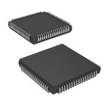 A40MX04-2PLG68

The activity of extra discounts on wholesale prices is in full swing…
Please fill in your contact information and we will send you the latest wholesale price list.



