 ChipApex | Global Electronic Components Supplier

SEARCH
Search Product
Search Post
— IC芯片 | 连接器 | 传感器 | 被动器件 —
Search productSearch post
— IC芯片 | 连接器 | 传感器 | 被动器件 —
Consult the customer manager about the wholesale price.
consultation hotline:86-132-6715-2157
email:[email protected]
Contact the product manager for consultation. One-stop consultation is available.
Do you want a lower wholesale price? Please send us your inquiry and we will reply immediately.
The A40MX04-3PL84I is a field-programmable gate array from the Microchip MX family, featuring 6,000 system gates and 547 logic elements. It provides 69 I/O pins within an 84-pin PLCC package. The device supports mixed-voltage operation at 3.3 V or 5.0 V with PCI-compliant I/Os. Operating temperatures range from -40°C to +85°C for industrial applications. Key specifications include up to 2.5 kbits of configurable dual-port SRAM, deterministic timing, and IEEE 1149.1 JTAG boundary scan support.
Verify current availability status directly with authorized distributors as lead times may vary. Confirm RoHS compliance and specific ordering suffixes match project requirements. Check for recent Product Change Notifications regarding packaging or assembly site updates before finalizing procurement plans.
Select this model for designs requiring 6K system gates with mixed 3.3V and 5V I/O compatibility. Ensure the PLCC-84 package fits the PCB footprint constraints. Consider the -3 speed grade for timing closure needs relative to higher-performance variants in the MX series.
This component belongs to the Actel (now Microchip) MX FPGA family, known for non-volatile flash-based technology. It serves as a drop-in replacement for complex PALs and GALs. The family emphasizes low power consumption and instant-on functionality without external configuration memory.
Direct pin-compatible substitutes within the same package are limited due to specific speed grades. Review the A40MX04 datasheet for other speed grades like -1 or -2 if timing requirements differ. Cross-family migration to newer Microchip PolarFire or SmartFusion devices requires schematic and layout redesign.

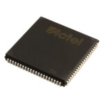 A40MX04-3PL84I

The activity of extra discounts on wholesale prices is in full swing…
Please fill in your contact information and we will send you the latest wholesale price list.



