 ChipApex | Global Electronic Components Supplier

SEARCH
Search Product
Search Post
— IC芯片 | 连接器 | 传感器 | 被动器件 —
Search productSearch post
— IC芯片 | 连接器 | 传感器 | 被动器件 —
Consult the customer manager about the wholesale price.
consultation hotline:86-132-6715-2157
email:[email protected]
Contact the product manager for consultation. One-stop consultation is available.
Do you want a lower wholesale price? Please send us your inquiry and we will reply immediately.
The A40MX04-PQG100 is a field-programmable gate array (FPGA) from the Microchip Technology MX series. It features 295 configurable logic blocks (CLBs) and approximately 2,000 system gates. The device supports up to 69 user-programmable I/O pins and operates with supply voltages of 3.3 V or 5 V. It is housed in a 100-pin PQFP package. Maximum clock frequency reaches 48.24 MHz with a CLB delay of 3.72 ns. Operating temperatures range from -55°C to +125°C for industrial/military grades.
Verify the specific suffix against official Microchip documentation to confirm voltage and temperature ratings. Confirm moisture sensitivity level (MSL 3) handling requirements during assembly. Check for active status as legacy parts may face end-of-life notices. Ensure ECAD models match the exact package variant.
Compare CLB count and I/O availability against design requirements. Evaluate speed grade (-1 vs -2 vs -3) for timing closure. Consider package options like PLCC or QFP based on board space. Verify compatibility with Actel Libero software tools for programming.
This component belongs to the A40MX family, designed as a single-chip ASIC alternative. It bridges the gap between complex CPLDs and larger FPGAs. The family emphasizes low power consumption and instant-on capability due to its flash technology base.
Direct substitutes include other A40MX variants with different packages or speed grades. Cross-reference pinouts when selecting PQFP versus PLCC alternatives. Verify functional equivalence if migrating from older Actel-branded components.


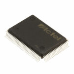 A40MX04-PQG100

The activity of extra discounts on wholesale prices is in full swing…
Please fill in your contact information and we will send you the latest wholesale price list.




