 ChipApex | Global Electronic Components Supplier

SEARCH
Search Product
Search Post
— IC芯片 | 连接器 | 传感器 | 被动器件 —
Search productSearch post
— IC芯片 | 连接器 | 传感器 | 被动器件 —
Consult the customer manager about the wholesale price.
consultation hotline:86-132-6715-2157
email:[email protected]
Contact the product manager for consultation. One-stop consultation is available.
Do you want a lower wholesale price? Please send us your inquiry and we will reply immediately.
The A42MX09-1PLG84 is a Field Programmable Gate Array (FPGA) from the Microchip MX family, housed in an 84-pin PLCC package. It features approximately 14,000 system gates and 72 I/O pins. The device operates on a single 5V supply voltage, with a specified range of 4.75V to 5.25V. It supports commercial temperature grades ranging from 0°C to +70°C. Key technical specifications include up to 2.5 kbits of configurable dual-port SRAM, fast wide-decode circuitry, and deterministic timing capabilities suitable for ASIC replacement designs.
Verify the specific suffix '1' against official Microchip documentation to confirm the exact temperature grade and speed bin, as variations exist within the A42MX09 series. Confirm current availability status, as many devices in this legacy MX family have reached end-of-life or obsolescence phases. Ensure compliance with RoHS directives if required for the target application environment.
Select this component when a 5V-only FPGA architecture is required for legacy system integration. The 84-pin PLCC package is suitable for through-hole mounting or specific socketed applications. Consider the 14,000 gate count and limited embedded memory when evaluating logic density requirements compared to higher-capacity members of the MX family.
This part belongs to the Microsemi/Microchip 40MX and 42MX FPGA families, which are established non-volatile flash-based technologies. These devices are engineered to consolidate logic previously implemented in multiple PALs, CPLDs, and FPGAs. The family emphasizes ease of integration and deterministic timing for industrial and automotive applications.
Direct substitutes may include other variants within the A42MX09 series with different packages, such as PQFP-144 or TQFP-176, provided pin compatibility is verified. Cross-family migration to newer Microchip PolarFire or IGLOO2 series requires significant architectural redesign due to differences in non-volatile technology and I/O standards.


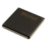 A42MX09-1PLG84

The activity of extra discounts on wholesale prices is in full swing…
Please fill in your contact information and we will send you the latest wholesale price list.




