 ChipApex | Global Electronic Components Supplier

SEARCH
Search Product
Search Post
— IC芯片 | 连接器 | 传感器 | 被动器件 —
Search productSearch post
— IC芯片 | 连接器 | 传感器 | 被动器件 —
Consult the customer manager about the wholesale price.
consultation hotline:86-132-6715-2157
email:[email protected]
Contact the product manager for consultation. One-stop consultation is available.
Do you want a lower wholesale price? Please send us your inquiry and we will reply immediately.
The A42MX09-PLG84A is a Field Programmable Gate Array (FPGA) from the Microchip A42MX series, housed in a PLCC-84 package. It features 336 Logic Elements and approximately 14,000 system gates. The device supports a minimum supply voltage of 4.75 V and a maximum of 5.25 V. It operates within a commercial temperature range of 0°C to +70°C. The FPGA provides up to 83 I/O pins and includes zero bits of embedded memory.
Verify the specific revision level and manufacturing date code against the latest Microchip datasheet before procurement. Confirm that the PLCC-84 package variant matches the required footprint for your PCB layout. Ensure compliance with RoHS directives if applicable to your assembly process. Check for any recent Product Change Notifications regarding component availability or material composition updates.
Select this model when a cost-effective 5V solution is required for consolidating logic previously implemented in multiple PALs or CPLDs. Consider the A42MX series for designs needing fast wide-decode circuitry and dual-port SRAM capabilities. Evaluate the 336 LE capacity against your logic density requirements to ensure optimal resource utilization without over-specifying the device.
This component belongs to the Microsemi (now Microchip) 40MX and 42MX FPGA families. These devices are designed as single-chip solutions to replace complex discrete logic. The family offers scalability from 3,000 to 54,000 system gates, providing flexibility for various digital design applications while maintaining compatibility with standard 5V power supplies.
Publicly confirmed substitute part numbers for this specific component were not identified in the available documentation.


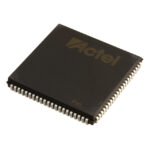 A42MX09-PLG84A

The activity of extra discounts on wholesale prices is in full swing…
Please fill in your contact information and we will send you the latest wholesale price list.



