 ChipApex | Global Electronic Components Supplier

SEARCH
Search Product
Search Post
— IC芯片 | 连接器 | 传感器 | 被动器件 —
Search productSearch post
— IC芯片 | 连接器 | 传感器 | 被动器件 —
Consult the customer manager about the wholesale price.
consultation hotline:86-132-6715-2157
email:[email protected]
Contact the product manager for consultation. One-stop consultation is available.
Do you want a lower wholesale price? Please send us your inquiry and we will reply immediately.
The A42MX16-1TQ176M is a Field Programmable Gate Array (FPGA) from the Microsemi MX family, designed as a high-capacity single-chip ASIC alternative. It features 24,000 system gates and 295 Configurable Logic Blocks (CLBs). The device supports mixed-voltage operation with core and I/O voltages of 3.3V or 5.0V, ensuring PCI-compliant compatibility. Key performance metrics include a maximum clock frequency of 48.24 MHz, a CLB delay of 3.72 ns, and a 5.6 ns clock-to-out time. It integrates up to 2.5 kbits of configurable dual-port SRAM and offers up to 140 user-programmable I/O pins in a 176-LQFP package.
Verify the specific suffix 'M' against official Microsemi documentation to confirm temperature range and qualification status, as standard variants may differ. Confirm RoHS compliance status, as some MX family devices are noted as non-compliant in historical records. Check for active production status or obsolescence notices prior to procurement.
Select this component when a single-chip solution is required to replace multiple PALs, CPLDs, or FPGAs. Ensure the design utilizes the available 295 CLBs and 2.5 kbits of embedded memory. Verify that the 176-pin LQFP package fits the board layout constraints and that the 48.24 MHz speed grade meets the system timing requirements.
This part belongs to the 40MX and 42MX FPGA families, which offer system gate counts ranging from 3,000 to 54,000. These devices are engineered to shorten design cycles by consolidating logic into a single chip. The family supports commercial, industrial, automotive, and military temperature grades, with options for ceramic packages and QML certification.
Direct substitutes within the same gate count and package include the A42MX16-1TQ176I or A42MX16-2TQ176I. Variants with different suffixes may indicate changes in temperature range or quality level rather than functional differences.


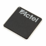 A42MX16-1TQ176M

The activity of extra discounts on wholesale prices is in full swing…
Please fill in your contact information and we will send you the latest wholesale price list.



