 ChipApex | Global Electronic Components Supplier

SEARCH
Search Product
Search Post
— IC芯片 | 连接器 | 传感器 | 被动器件 —
Search productSearch post
— IC芯片 | 连接器 | 传感器 | 被动器件 —
Consult the customer manager about the wholesale price.
consultation hotline:86-132-6715-2157
email:[email protected]
Contact the product manager for consultation. One-stop consultation is available.
Do you want a lower wholesale price? Please send us your inquiry and we will reply immediately.
The A42MX16-3TQ176I is a Field Programmable Gate Array (FPGA) from the Microsemi MX family, housed in a 176-LQFP surface-mount package. It provides 24,000 system gates and supports up to 140 user-programmable I/O pins. The device operates on mixed-voltage supplies of 3.3V or 5.0V for both core and I/Os. Key performance metrics include a maximum clock frequency of 250 MHz, a 5.6 ns clock-to-out delay, and 5 ns dual-port SRAM access time. It integrates up to 2.5 kbits of configurable dual-port SRAM and features fast wide-decode circuitry with 7.5 ns address decode capability.
Verify component authenticity through authorized channels due to discontinuation status. Confirm RoHS compliance requirements as older stock may not meet current environmental standards. Check for moisture sensitivity level 3 handling precautions during storage and assembly. Validate package integrity against shipping damage risks associated with LQFP formats.
Select this model when 24,000 system gates and 140 I/Os are required within a 176-pin footprint. Ensure design compatibility with 3.3V or 5.0V mixed-voltage domains. Consider the 250 MHz performance limit for high-speed logic applications. Verify that the 176-LQFP package fits the target PCB layout constraints.
This part belongs to the Microsemi 40MX and 42MX FPGA families, designed as single-chip ASIC alternatives. These devices consolidate logic previously implemented in multiple PALs, CPLDs, and FPGAs. The MX series targets cost-effective designs with high performance, shortening development cycles for complex digital systems requiring flexible programmability.
Publicly confirmed substitute part numbers are not available in the provided documentation. Users should consult Microchip Technology for current lifecycle notifications and recommended obsolescence management strategies.


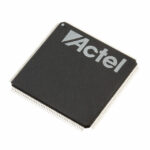 A42MX16-3TQ176I

The activity of extra discounts on wholesale prices is in full swing…
Please fill in your contact information and we will send you the latest wholesale price list.




