 ChipApex | Global Electronic Components Supplier

SEARCH
Search Product
Search Post
— IC芯片 | 连接器 | 传感器 | 被动器件 —
Search productSearch post
— IC芯片 | 连接器 | 传感器 | 被动器件 —
Consult the customer manager about the wholesale price.
consultation hotline:86-132-6715-2157
email:[email protected]
Contact the product manager for consultation. One-stop consultation is available.
Do you want a lower wholesale price? Please send us your inquiry and we will reply immediately.
The A42MX16-FVQG100 is a high-capacity Field Programmable Gate Array (FPGA) from the Microchip MX family, designed as a single-chip ASIC alternative. It features 295 Configurable Logic Blocks (CLBs) and approximately 2,000 system gates. The device supports mixed-voltage operation with core and I/O voltages of 3.3V or 5.0V, ensuring PCI-compliant compatibility. Key performance metrics include a maximum clock frequency of 48.24 MHz, a 5.6 ns clock-to-out delay, and 5 ns dual-port SRAM access time. It integrates up to 2.5 kbits of configurable dual-port SRAM and offers up to 83 user-programmable I/O pins in a 100-pin FineLine BGA package.
Verify the specific suffix 'FVQG100' against official Microchip documentation to confirm package type and temperature grade. Ensure compliance with RoHS3 standards and check Moisture Sensitivity Level (MSL) requirements for handling. Confirm availability through authorized distributors, as lead times may vary based on manufacturing schedules.
Select this model for applications requiring deterministic timing and high pin-locking ratios. Compare CLB counts and gate densities against similar MX series devices if lower complexity is sufficient. Verify voltage levels match the target system's I/O requirements to ensure seamless integration without additional level shifting.
This component belongs to the Microsemi (now Microchip Technology) 40MX and 42MX FPGA families. These devices are engineered for cost-effective design solutions that shorten development cycles. The family provides scalable options ranging from 3,000 to 54,000 system gates, catering to diverse embedded logic needs across commercial and industrial sectors.
Direct replacements within the same package and functionality include other variants from the A42MX16 series, such as A42MX16-VQG100A or A42MX16-PQ100A, depending on the required package style. Cross-family migration to newer Actel or SmartFusion devices may require significant redesign.
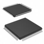 A42MX16-FVQG100

The activity of extra discounts on wholesale prices is in full swing…
Please fill in your contact information and we will send you the latest wholesale price list.






