 ChipApex | Global Electronic Components Supplier

SEARCH
Search Product
Search Post
— IC芯片 | 连接器 | 传感器 | 被动器件 —
Search productSearch post
— IC芯片 | 连接器 | 传感器 | 被动器件 —
Consult the customer manager about the wholesale price.
consultation hotline:86-132-6715-2157
email:[email protected]
Contact the product manager for consultation. One-stop consultation is available.
Do you want a lower wholesale price? Please send us your inquiry and we will reply immediately.
The A42MX16-PLG84I is a Field Programmable Gate Array (FPGA) from the Microchip MX Automotive Family. It provides 24,000 system gates and supports mixed-voltage operation at 3.3V or 5.0V for core and I/Os. The device features up to 2.5 kbits of configurable dual-port SRAM and fast wide-decode circuitry. It operates within an industrial temperature range of -40°C to +85°C and utilizes an 84-pin PLCC package with 72 user-programmable I/O pins.
Verify RoHS compliance status carefully, as specific suffixes in this family may indicate non-compliance. Confirm the exact package type and temperature grade against the manufacturer's current datasheet before procurement, as availability and environmental certifications can vary by production batch.
Select this model for designs requiring 24,000 system gates with mixed 3.3V/5V I/O capabilities. Ensure the design fits within the 72 available I/O pins and 2.5 kbits SRAM limit. Verify that the PLCC package form factor matches the PCB footprint requirements and that the -40°C to +85°C operating range meets the application's thermal constraints.
This component belongs to the Microchip MX Automotive Family of FPGAs, which offers cost-effective solutions for consolidating complex logic. The series ranges from 3,000 to 54,000 system gates, providing high performance while shortening development cycles compared to discrete logic implementations.
Check for direct substitutes within the A42MX16 series with different packages, such as A42MX16-PQG100I or A42MX16-2TQG176I, if pin compatibility allows. Verify functional equivalence regarding gate count and SRAM capacity when considering cross-package replacements.
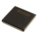 A42MX16-PLG84I

The activity of extra discounts on wholesale prices is in full swing…
Please fill in your contact information and we will send you the latest wholesale price list.






