 ChipApex | Global Electronic Components Supplier

SEARCH
Search Product
Search Post
— IC芯片 | 连接器 | 传感器 | 被动器件 —
Search productSearch post
— IC芯片 | 连接器 | 传感器 | 被动器件 —
Consult the customer manager about the wholesale price.
consultation hotline:86-132-6715-2157
email:[email protected]
Contact the product manager for consultation. One-stop consultation is available.
Do you want a lower wholesale price? Please send us your inquiry and we will reply immediately.
The A42MX16-PQ100 is a Field Programmable Gate Array (FPGA) from the Microchip MX family, housed in a 100-pin Plastic Quad Flat Package (PQFP). It provides approximately 24,000 system gates and 608 Logic Elements. The device supports mixed-voltage operation with core and I/O voltages of 3.3V or 5.0V, featuring up to 83 user-programmable I/O pins. Key performance metrics include a maximum clock frequency of 48.24 MHz and a CLB delay of 3.72 ns. It integrates configurable dual-port SRAM and fast wide-decode circuitry for high-capacity single-chip ASIC replacement.
Verify the specific suffix code against official datasheets to confirm voltage range and temperature grade. Standard commercial variants typically operate between -40°C and +85°C, while industrial or military grades extend to -55°C or +125°C. Confirm package authenticity as PQFP-100 and check for moisture sensitivity level requirements during storage and handling procedures.
Select this component when designing systems requiring moderate logic density with deterministic timing constraints. Ensure the design utilizes the available 83 I/O pins within the 100-pin footprint limits. Verify that the target application voltage aligns with the 3.3V or 5.0V support capabilities. Consider the 24k gate count for complex state machines or interface bridging tasks.
This part belongs to the Microsemi/Actel MX FPGA family, known for non-volatile flash-based technology. The A42MX16 variant specifically targets cost-effective ASIC alternatives. It consolidates logic functions previously handled by multiple programmable devices, reducing board space and power consumption in embedded control applications.
Direct substitutes include other parts within the A42MX16 series with different suffixes indicating package or temperature variations, such as A42MX16-PQG100A or A42MX16-VQG100A. Cross-family replacements like the A40MX series may require significant schematic and firmware redesign due to architectural differences.
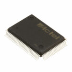 A42MX16-PQ100

The activity of extra discounts on wholesale prices is in full swing…
Please fill in your contact information and we will send you the latest wholesale price list.






