 ChipApex | Global Electronic Components Supplier

SEARCH
Search Product
Search Post
— IC芯片 | 连接器 | 传感器 | 被动器件 —
Search productSearch post
— IC芯片 | 连接器 | 传感器 | 被动器件 —
Consult the customer manager about the wholesale price.
consultation hotline:86-132-6715-2157
email:[email protected]
Contact the product manager for consultation. One-stop consultation is available.
Do you want a lower wholesale price? Please send us your inquiry and we will reply immediately.
The A42MX16-PQG100 is a Field Programmable Gate Array (FPGA) from the Microchip MX family, housed in a PQFP-100 package. It provides 24,000 system gates and 608 Logic Elements (LEs). The device supports mixed-voltage operation with supply voltages ranging from 3V to 5.5V. It features 83 user-programmable I/O pins and operates within temperature ranges of -40°C to +85°C for industrial variants. The FPGA includes up to 2.5 kbits of configurable dual-port SRAM and offers deterministic timing with up to 100% resource utilization and pin locking capabilities.
Verify the specific suffix against official Microchip documentation to confirm temperature grade and speed variant. Ensure compatibility with design tools such as Libero SoC. Check for moisture sensitivity level requirements during storage and handling. Confirm RoHS compliance status for the specific revision. Validate package dimensions against PCB footprint specifications.
Select this model for applications requiring high-density programmable logic in a QFP package. Consider the 24,000 gate capacity for complex state machines or data path processing. Evaluate the mixed-voltage I/O options if interfacing with different logic families. Verify that the 83 available I/O pins meet the interface requirements of the target system architecture.
This component belongs to the Microsemi/Actel MX FPGA family, known for non-volatile flash-based technology. The A42MX16 variant specifically targets mid-range complexity designs. It serves as a drop-in replacement for legacy discrete logic solutions. The PQG100 suffix indicates a plastic quad flat pack package with 100 leads.
Direct substitutes include other A42MX16 variants with different speed grades or temperature ratings, such as A42MX16-PQG100I or A42MX16-PQG100A. Cross-family migration to A54SX16 may require significant design rework due to architectural differences.
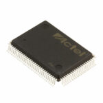 A42MX16-PQG100

The activity of extra discounts on wholesale prices is in full swing…
Please fill in your contact information and we will send you the latest wholesale price list.





