 ChipApex | Global Electronic Components Supplier

SEARCH
Search Product
Search Post
— IC芯片 | 连接器 | 传感器 | 被动器件 —
Search productSearch post
— IC芯片 | 连接器 | 传感器 | 被动器件 —
Consult the customer manager about the wholesale price.
consultation hotline:86-132-6715-2157
email:[email protected]
Contact the product manager for consultation. One-stop consultation is available.
Do you want a lower wholesale price? Please send us your inquiry and we will reply immediately.
The A42MX24-2PL84 is a Field Programmable Gate Array (FPGA) from the Microchip MX Automotive Family. It features 36,000 system gates and 912 logic elements within a PLCC-84 package. The device supports mixed-voltage operation at 3.3 V or 5 V core supplies with PCI-compliant I/Os. It includes up to 2.5 kbits of configurable dual-port SRAM and fast wide-decode circuitry. Key specifications include deterministic timing, user-controllable delays, and IEEE 1149.1 JTAG boundary scan support for verification.
Verify component authenticity through authorized Microchip distributors or direct manufacturer channels. Confirm RoHS compliance status as specific variants may differ. Check for End-of-Life notifications or Product Change Notices regarding discontinuation. Ensure supply chain stability given the mature nature of this FPGA family.
Select the A42MX24-2PL84 when 36,000 system gates and 72 I/O pins are required in a PLCC-84 footprint. Consider this part for designs needing mixed 3.3V/5V I/O compatibility. Evaluate thermal performance within the specified operating temperature range. Compare against higher-capacity models if additional logic resources are anticipated.
This component belongs to the Actel/Microchip MX series of flash-based FPGAs. These devices are designed to replace complex discrete logic or custom ASICs. The MX family emphasizes low power consumption and non-volatile configuration storage without external memory requirements.
Publicly confirmed substitute part numbers for the A42MX24-2PL84 are not available in the provided documentation. Users should consult Microchip's official obsolescence notices or engineering support for recommended migration paths to current FPGA families.


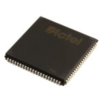 A42MX24-2PL84

The activity of extra discounts on wholesale prices is in full swing…
Please fill in your contact information and we will send you the latest wholesale price list.




