 ChipApex | Global Electronic Components Supplier

SEARCH
Search Product
Search Post
— IC芯片 | 连接器 | 传感器 | 被动器件 —
Search productSearch post
— IC芯片 | 连接器 | 传感器 | 被动器件 —
Consult the customer manager about the wholesale price.
consultation hotline:86-132-6715-2157
email:[email protected]
Contact the product manager for consultation. One-stop consultation is available.
Do you want a lower wholesale price? Please send us your inquiry and we will reply immediately.
The A42MX24-2PLG84I is a Flash-based Field Programmable Gate Array (FPGA) from the Microchip MX Automotive family, designed as a single-chip ASIC alternative. It features 36,000 system gates and 912 Logic Elements within a PLCC-84 package. The device supports mixed-voltage operation with core voltages of 3.3V or 5V and I/O voltages ranging from 4.75V to 5.25V. It includes up to 2.5 kbits of configurable dual-port SRAM and offers deterministic timing with user-controllable delays. The component operates within an industrial temperature range of 0°C to +70°C and supports IEEE 1149.1 JTAG boundary scan testing.
Verify the specific suffix 'I' against official Microchip documentation to confirm industrial temperature grade specifications. Confirm current production status as discontinuance notices may affect long-term availability. Ensure compatibility with existing PCB footprints for the PLCC-84 package before procurement.
Select this model when a Flash-based FPGA with instant-on capability is required for automotive or industrial environments. Compare gate counts and I/O flexibility against other MX series devices if higher capacity is needed. Verify voltage requirements match the target system's 3.3V or 5V logic levels.
This component belongs to the A42MX24 series within the broader MX FPGA portfolio. It shares architectural similarities with other Flash FPGAs but is distinguished by its specific gate density and PLCC-84 packaging. The series is positioned as a robust solution for replacing complex discrete logic or ASICs in harsh environments.
Check for direct pin-compatible upgrades within the A42MX series, such as the A42MX36, if additional logic resources are required. Verify that any substitute maintains the same PLCC-84 package and voltage specifications to ensure mechanical and electrical compatibility.
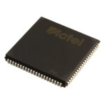 A42MX24-2PLG84I

The activity of extra discounts on wholesale prices is in full swing…
Please fill in your contact information and we will send you the latest wholesale price list.





