 ChipApex | Global Electronic Components Supplier

SEARCH
Search Product
Search Post
— IC芯片 | 连接器 | 传感器 | 被动器件 —
Search productSearch post
— IC芯片 | 连接器 | 传感器 | 被动器件 —
Consult the customer manager about the wholesale price.
consultation hotline:86-132-6715-2157
email:[email protected]
Contact the product manager for consultation. One-stop consultation is available.
Do you want a lower wholesale price? Please send us your inquiry and we will reply immediately.
The A42MX24-PL84A is a Field Programmable Gate Array (FPGA) from the Microchip MX Automotive Family, designed as a single-chip ASIC alternative for automotive applications. It features 36,000 system gates and 912 Configurable Logic Blocks (CLBs). The device utilizes CMOS technology and is housed in an 84-pin Plastic Quad Flat Package (PQCC84), also identified as LCC-84. It supports mixed-voltage operation with 5.0V or 3.3V supplies for core and I/Os, ensuring PCI-compliant interface compatibility. Key architectural elements include up to 2.5 kbits of configurable dual-port SRAM, fast wide-decode circuitry, and deterministic user-controllable timing.
Verify component authenticity through authorized Microchip Technology distributors. Confirm RoHS compliance status, as specific suffixes may indicate non-compliant variants. Check for discontinuation notices, as older MX family parts may have limited availability. Ensure packaging specifications match the required PQCC84 form factor for PCB integration.
Select this model when 36,000 system gates and 912 CLBs are sufficient for the logic density requirements. Consider the PL84 package only if an 84-pin footprint is mandatory. Evaluate the 5.0V/3.3V mixed-voltage support against interface voltage levels. Compare against other MX family members like A42MX09 or A42MX36 if gate counts or I/O pins differ significantly.
This component belongs to the Microchip MX FPGA family, which bridges the gap between standard programmable logic and custom ASICs. The series is characterized by its flash-based non-volatile technology, enabling instant-on functionality. The A42MX24 variant specifically targets mid-range complexity designs within industrial and automotive sectors.
Direct substitutes include other A42MX24 variants with different packages or temperature grades, such as A42MX24-PQ208A or A42MX24-PL84I. Verify that any replacement maintains the same 36,000 gate count and 84-pin configuration to ensure mechanical and logical compatibility.
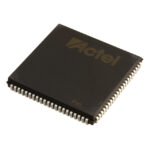 A42MX24-PL84

The activity of extra discounts on wholesale prices is in full swing…
Please fill in your contact information and we will send you the latest wholesale price list.






